ICP Etching Recipes: Difference between revisions
→Process Tips: added oil mounting tips to each tool |
→High Rate Bosch Etch (DSEIII): update about plasma dicing recipe |
||
| (3 intermediate revisions by the same user not shown) | |||
| Line 20: | Line 20: | ||
==High Rate Bosch Etch (DSEIII)== |
==High Rate Bosch Etch (DSEIII)== |
||
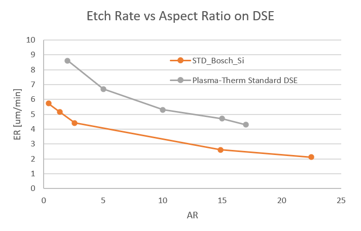
*[//wiki.nanotech.ucsb.edu/wiki/images/4/4a/10-Si_Etch_Bosch_DSEIII.pdf Bosch Process Recipe and Characterization] - Standard recipe on the tool.[[File:DSEiii Bosch Ecth SEM Example 01.png|alt=Example SEM image|thumb|188x188px|Example of 100µm Deep Bosch Etched Silicon posts with hard mask. Close inspection shows the horizontal "scalloping" from the cycling nature of the etch. (Image Credit: [[Demis D. John]], 2021-07)]] |
*[//wiki.nanotech.ucsb.edu/wiki/images/4/4a/10-Si_Etch_Bosch_DSEIII.pdf Bosch Process Recipe and Characterization] - Standard recipe on the tool.[[File:DSEiii Bosch Ecth SEM Example 01.png|alt=Example SEM image|thumb|188x188px|Example of 100µm Deep Bosch Etched Silicon posts with Al<sub>2</sub>O<sub>3</sub> hard mask. Close inspection shows the horizontal "scalloping" from the cycling nature of the etch. (Image Credit: [[Demis D. John]], 2021-07)]] |
||
**'''STD_Bosch_Si (⭐️Production)''' - Developed 2024-10 |
**'''STD_Bosch_Si (⭐️Production)''' - Developed 2024-10 |
||
***Old Recipe Name: "'''''Plasma-Therm Standard DSE'''''" - lower EtchA, less tolerant |
***Old Recipe Name: "'''''Plasma-Therm Standard DSE'''''" - lower EtchA, less tolerant |
||
| Line 39: | Line 39: | ||
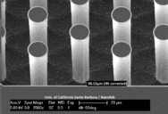
|[[File:DSE_16um_Bosch_Etch_-_22_013.jpg|alt=Example SEM image|none|thumb|250x250px|Example of 16.32µm Deep Etched Silicon with 650nm thick UV6 Photoresist mask, 2µm Pitch. (''Image Credit: [[Noah Dutra]] 2024-08'')]] |
|[[File:DSE_16um_Bosch_Etch_-_22_013.jpg|alt=Example SEM image|none|thumb|250x250px|Example of 16.32µm Deep Etched Silicon with 650nm thick UV6 Photoresist mask, 2µm Pitch. (''Image Credit: [[Noah Dutra]] 2024-08'')]] |
||
|} |
|} |
||
:: |
|||
=== '''Si Etching C<sub>4</sub>F<sub>8</sub>/SF<sub>6</sub>/Ar (PlasmaTherm DSEiii)''' === |
|||
[[File:DSE plot.png|alt=example of Process Control Charts|thumb|[https://docs.google.com/spreadsheets/d/1xQcdUH560nT928miZMeP7xxQSwHz_a_EB9s_Kb1LSfg/edit?gid=1804752281#gid=1804752281 Click for Process Control Charts]|link=https://docs.google.com/spreadsheets/d/1xQcdUH560nT928miZMeP7xxQSwHz_a_EB9s_Kb1LSfg/edit?gid=1804752281#gid=1804752281|232x232px]] |
|||
* Recipe: ''STD_Bosch_Si (⭐️Production),'' on 100mm Si Wafer with ~50% open area, photoresist mask, ~40µm deep |
|||
*[https://docs.google.com/spreadsheets/d/1xQcdUH560nT928miZMeP7xxQSwHz_a_EB9s_Kb1LSfg/edit?gid=0#gid=0 Si Etching with C<sub>4</sub>F<sub>8</sub>/SF<sub>6</sub>/Ar - '''Etch Data'''] |
|||
*[https://docs.google.com/spreadsheets/d/1xQcdUH560nT928miZMeP7xxQSwHz_a_EB9s_Kb1LSfg/edit?gid=1804752281#gid=1804752281 Si Etching with C<sub>4</sub>F<sub>8</sub>/SF<sub>6</sub>/Ar - '''Plots'''] |
|||
===Through Silicon Via (TSV) etch (DSEiii)=== |
===Through Silicon Via (TSV) etch (DSEiii)=== |
||
| Line 46: | Line 52: | ||
Instead, we recommend the following process with Al<sub>2</sub>O<sub>3</sub> hardmask: |
Instead, we recommend the following process with Al<sub>2</sub>O<sub>3</sub> hardmask: |
||
<big>'''NOTE''': We have recently found that the wax-mounting process process can leave wax on the wafer clamp, causing the next user's wafer to get stuck and fail transfer! '''<u>DO NOT RUN</u>''' the wax-mounting process without discussing with staff first. ''(Through-wafer process with no wax is still acceptable.)'' -- [[Demis D. John|Demis]] 2024-03-11</big> |
<big>'''NOTE''': We have recently found that the wax-mounting process process can leave wax on the wafer clamp, causing the next user's wafer to get stuck and fail transfer! '''<u>DO NOT RUN</u>''' the wax-mounting process without discussing with staff first. ''(Through-wafer process with no wax is still acceptable.)'' -- [[Demis D. John|Demis]] 2024-03-11</big> |
||
Staff is working on a dicing-tape mounted recipe, to be published here soon. |
|||
-- [[Demis D. John|Demis]] 2025-11-19 |
|||
{| class="wikitable" |
{| class="wikitable" |
||
! colspan="2" |Process for Through-Wafer Silicon Etching |
! colspan="2" |Process for Through-Wafer Silicon Etching |
||
| Line 131: | Line 140: | ||
**Used instead of Bosch Process, to avoid scalloping on the sidewall. |
**Used instead of Bosch Process, to avoid scalloping on the sidewall. |
||
**Lower selectivity, lower etch rate, smoother sidewalls. |
**Lower selectivity, lower etch rate, smoother sidewalls. |
||
==Process Control Data (DSEiii)== |
|||
'''Si Etching C<sub>4</sub>F<sub>8</sub>/SF<sub>6</sub>/Ar (PlasmaTherm DSEiii)''' |
|||
* Recipe: ''STD_Bosch_Si (⭐️Production),'' on 100mm Si Wafer with ~50% open area, photoresist mask, ~40µm deep |
|||
*[https://docs.google.com/spreadsheets/d/1xQcdUH560nT928miZMeP7xxQSwHz_a_EB9s_Kb1LSfg/edit?gid=0#gid=0 Si Etching with C<sub>4</sub>F<sub>8</sub>/SF<sub>6</sub>/Ar - '''Etch Data'''] |
|||
*[https://docs.google.com/spreadsheets/d/1xQcdUH560nT928miZMeP7xxQSwHz_a_EB9s_Kb1LSfg/edit?gid=1804752281#gid=1804752281 Si Etching with C<sub>4</sub>F<sub>8</sub>/SF<sub>6</sub>/Ar - '''Plots'''][[File:DSE plot.png|alt=example of Process Control Charts|none|thumb|[https://docs.google.com/spreadsheets/d/1xQcdUH560nT928miZMeP7xxQSwHz_a_EB9s_Kb1LSfg/edit?gid=1804752281#gid=1804752281 Click for Process Control Charts]|link=https://docs.google.com/spreadsheets/d/1xQcdUH560nT928miZMeP7xxQSwHz_a_EB9s_Kb1LSfg/edit?gid=1804752281#gid=1804752281]] |
|||
=[[Fluorine ICP Etcher (PlasmaTherm/SLR Fluorine ICP)|PlasmaTherm/SLR Fluorine Etcher]]= |
=[[Fluorine ICP Etcher (PlasmaTherm/SLR Fluorine ICP)|PlasmaTherm/SLR Fluorine Etcher]]= |
||
| Line 175: | Line 176: | ||
*We have observed that full-wafers with small open area in ''photoresist masks'' might require a recalibration of the C4F8/SF6 ratio in order to prevent very low etch rates. |
*We have observed that full-wafers with small open area in ''photoresist masks'' might require a recalibration of the C4F8/SF6 ratio in order to prevent very low etch rates. |
||
== |
=== Process Control: Si Etching C<sub>4</sub>F<sub>8</sub>/SF<sub>6</sub>/CF<sub>4</sub> (Fluorine ICP Etcher) === |
||
[[File:FICP-Si.png|alt=example of Process Control Charts|thumb|242x242px|[https://docs.google.com/spreadsheets/d/15iRs-JhfgkMto5rZVtG0hJjcLMiHy039_ahv2nus0UQ/edit?gid=1804752281#gid=1804752281 Click for Process Control Charts]|link=https://docs.google.com/spreadsheets/d/15iRs-JhfgkMto5rZVtG0hJjcLMiHy039_ahv2nus0UQ/edit?gid=1804752281#gid=1804752281]]''Full Wafer Si etching with ~50% open area and resist mask, run weekly by [[Process Group Interns|NanoFab Interns]].'' |
|||
*[https://docs.google.com/spreadsheets/d/15iRs-JhfgkMto5rZVtG0hJjcLMiHy039_ahv2nus0UQ/edit?gid=0#gid=0 Si Etching with C<sub>4</sub>F<sub>8</sub>/SF<sub>6</sub>/CF<sub>4</sub> - '''Etch Data'''] |
|||
*'''"SiO2 Etch-50W" (⭐️Production)''' |
|||
*[https://docs.google.com/spreadsheets/d/15iRs-JhfgkMto5rZVtG0hJjcLMiHy039_ahv2nus0UQ/edit?gid=1804752281#gid=1804752281 Si Etching with C<sub>4</sub>F<sub>8</sub>/SF<sub>6</sub>/CF<sub>4</sub> - '''Plots'''] |
|||
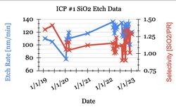
==SiO2 Etch Recipes (Fluorine ICP Etcher)== |
|||
[[File:FL-ICP_50W_SiO2_etch_with_Ru_Hard_Mask.png|alt=SEM of FL-ICP 50W SiO2 etch with Ru Hard Mask|thumb|266x266px|50W SiO2 Etch w/ Ru Hardmask]] |
|||
[[File:FL-ICP_200W_SiO2_Etch_with_Ru_Hardmask_-_Ning_Cao.png|alt=SEM of FL-ICP 200W SiO2 Etch with Ru Hardmask - Ning Cao|thumb|266x266px|200W SiO2 Etch w/ Ru Hardmask (Ning Cao)]] |
|||
*'''"SiO<sub>2</sub> Etch-50W" (⭐️Production)''' |
|||
**3.8mT, RF=50W, ICP=900W, CHF3/CF4=10/30sccm |
**3.8mT, RF=50W, ICP=900W, CHF3/CF4=10/30sccm |
||
**SiO<sub>2</sub> etch rate: ~250nm/min |
**SiO<sub>2</sub> etch rate: ~250nm/min |
||
| Line 183: | Line 191: | ||
**Selectivity SiO<sub>2</sub>:Ru ≈ 36 |
**Selectivity SiO<sub>2</sub>:Ru ≈ 36 |
||
**[[ICP Etching Recipes#SiO2 Etching with CHF3/CF4 (Fluorine ICP Etcher)|Process Control Data Above]] - Staff/Intern-run Etches Weekly, tracked over time. |
**[[ICP Etching Recipes#SiO2 Etching with CHF3/CF4 (Fluorine ICP Etcher)|Process Control Data Above]] - Staff/Intern-run Etches Weekly, tracked over time. |
||
*[//wiki.nanotech.ucsb.edu/w/images/f/f6/SiO2_Etch%2C_Ru_HardMask_-_Fluorine_ICP_Etch_Process_-_Ning_Cao_2019-06.pdf SiO2 Etching using Ruthenium Hardmask] - Full Process Traveler |
|||
=== [//wiki.nanotech.ucsb.edu/w/images/f/f6/SiO2_Etch%2C_Ru_HardMask_-_Fluorine_ICP_Etch_Process_-_Ning_Cao_2019-06.pdf SiO<sub>2</sub> Etching using Ruthenium Hardmask] === |
|||
**''Ning Cao & Bill Mitchell, 2019-06'' |
|||
**''High-selectivity and deep etching using sputtered Ru hardmask and I-Line litho.'' |
|||
* Click above for [http://wiki.nanotech.ucsb.edu/w/images/f/f6/SiO2_Etch%2C_Ru_HardMask_-_Fluorine_ICP_Etch_Process_-_Ning_Cao_2019-06.pdf Full Process Traveler] |
|||
**''Etch also works well with PR masking'' |
|||
** Process written for Sputtered Ru & I-Line GCA Stepper litho |
|||
**''Chemistry: CHF3/CF4'' |
|||
** Can be transferred to ALD Ru or DUV/EBL Litho. |
|||
**''Variations in SiO<sub>2</sub> etch Bias Power: 50 / 200 / 400W bias.'' |
|||
**Ru etch selectivity to PR: 0.18 (less than 1): 150nm Ru / 800nm PR |
|||
*''Ning Cao & Bill Mitchell, 2019-06'' |
|||
**50W Bias: ('''recommended''') |
|||
*''High-selectivity and deep etching using sputtered Ru hardmask and I-Line litho.'' |
|||
***Selectivity to photoresist: 1.10–1.20 |
|||
*''Etch also works well with PR masking'' |
|||
***SiO<sub>2</sub> selectivity to Ru: 36 |
|||
*''Chemistry: CHF3/CF4'' |
|||
***SiO<sub>2</sub> etch rate: 263nm/min |
|||
*''Variations in SiO<sub>2</sub> etch Bias Power: 50 / 200 / 400W bias.'' |
|||
**200W Bias: |
|||
* |
*Ru etch selectivity to PR: 0.18 (less than 1): 150nm Ru / 800nm PR |
||
*50W Bias: ('''recommended''') |
|||
***SiO<sub>2</sub> etch rate: 471nm/min |
|||
**Selectivity to photoresist: 1.10–1.20 |
|||
**This etch is detailed in the following article: [[Template:Publications#Highly Selective and Vertical Etch of Silicon Dioxide using Ruthenium Films as an Etch Mask|W.J. Mitchell ''et al.'', JVST-A, May 2021]] |
|||
**SiO<sub>2</sub> selectivity to Ru: 36 |
|||
{| class="wikitable" |
|||
**SiO<sub>2</sub> etch rate: 263nm/min |
|||
!50W SiO2 Etch w/ Ru Hardmask |
|||
**''Smoothest vertical etch for SiO2.'' |
|||
!200W SiO2 Etch w/ Ru Hardmask (Ning Cao) |
|||
*200W Bias: (higher etch rate) |
|||
|- |
|||
**SiO<sub>2</sub> selectivity to Ru: 38 |
|||
|[[File:FL-ICP 50W SiO2 etch with Ru Hard Mask.png|alt=SEM of FL-ICP 50W SiO2 etch with Ru Hard Mask|266x266px]] |
|||
**SiO<sub>2</sub> etch rate: 471nm/min |
|||
|[[File:FL-ICP 200W SiO2 Etch with Ru Hardmask - Ning Cao.png|alt=SEM of FL-ICP 200W SiO2 Etch with Ru Hardmask - Ning Cao|266x266px]] |
|||
*This etch is detailed in the following article: [[Template:Publications#Highly Selective and Vertical Etch of Silicon Dioxide using Ruthenium Films as an Etch Mask|W.J. Mitchell ''et al.'', JVST-A, May 2021]] |
|||
|} |
|||
*Updates: Many users have found that SiO2-masking the Ru hardmask results in vastly improved photoresist selectivity, making litho+etch of small features much better. |
|||
**Layer stack looks like: SiO2 (or other dielectric target layer to etch) / Ru hardmask / SiO2 hardmask (thin) / Photoresist. |
|||
**Typically strip the masks+PR with all dry etching. That means the entire etch process (all etches and strips) can be run ''in situ'' on the Panasonic ICP in a rapid single-tool etch process. |
|||
===Process Control: SiO<sub>2</sub> Etching with CHF3/CF4 (Fluorine ICP Etcher)=== |
|||
[[File:FL-ICP Process Control Data Example.jpg|alt=example of Process Control Charts|thumb|242x242px|[https://docs.google.com/spreadsheets/d/15hYkCqL3UNNayt4sXrvVi4mBj-OSdnF7PE29mQW9AEY/edit#gid=1804752281 Click for Process Control Charts]|link=https://docs.google.com/spreadsheets/d/15hYkCqL3UNNayt4sXrvVi4mBj-OSdnF7PE29mQW9AEY/edit#gid=1804752281]]''Full Wafer Si etching with ~50% open area and resist mask, run weekly by [[Process Group Interns|NanoFab Interns]].'' |
|||
*[https://docs.google.com/spreadsheets/d/15hYkCqL3UNNayt4sXrvVi4mBj-OSdnF7PE29mQW9AEY/edit?usp=sharing SiO<sub>2</sub> Etching with CHF3/CF4 - '''Etch Data'''] |
|||
*[https://docs.google.com/spreadsheets/d/15hYkCqL3UNNayt4sXrvVi4mBj-OSdnF7PE29mQW9AEY/edit#gid=1804752281 SiO<sub>2</sub> Etching with CHF3/CF4 - '''Plots'''] |
|||
==Si<sub>3</sub>N<sub>4</sub> Etching (Fluorine ICP Etcher)== |
==Si<sub>3</sub>N<sub>4</sub> Etching (Fluorine ICP Etcher)== |
||
| Line 224: | Line 239: | ||
**~60nm thick (2500krpm) |
**~60nm thick (2500krpm) |
||
**O2=20sccm / 10mT / RF1(bias)=100W / RF2(icp)=0W |
**O2=20sccm / 10mT / RF1(bias)=100W / RF2(icp)=0W |
||
**1min |
**45sec-1min |
||
[[File:SEM Image of wafer after PR strip.png|thumb|294x294px|Wafer had UV6 or UVN30 as mask. 5min Si etch followed by '''PostBARC Etch/PR Strip (STD)''' with 2min over etch]] |
[[File:SEM Image of wafer after PR strip.png|thumb|294x294px|<u>Original PR strip recipe</u>: Wafer had UV6 or UVN30 as mask. 5min Si etch followed by '''PostBARC Etch/PR Strip (STD)''' with 2min over etch (Credit: [[Gopikrishnan G M|Gopi Meena]])]] |
||
=== Photoresist Strip/Polymer Removal (Fluorine ICP Etcher) === |
=== Photoresist Strip/Polymer Removal (Fluorine ICP Etcher) === |
||
| Line 234: | Line 249: | ||
*Not able to completely remove PR (both negative & positive) after prolonged over etching (over etching of +2min) |
*Not able to completely remove PR (both negative & positive) after prolonged over etching (over etching of +2min) |
||
*Leaves behind residue on the sides |
*Leaves behind residue on the sides |
||
[[File:SEM Image.png|thumb|Wafer had UV6 or UVN30 as mask. 5min Si etch followed by '''PostBARC Etch/PR Strip (STD)_V2''' with 2min over etch]] |
[[File:SEM Image.png|thumb|<u>New PR Strip recipe</u>: Wafer had UV6 or UVN30 as mask. 5min Si etch followed by '''PostBARC Etch/PR Strip (STD)_V2''' with 2min over etch (Credit: [[Gopikrishnan G M|Gopi Meena]])]] |
||
'''New''' PR strip recipe: '''PostBARC Etch/PR Strip (STD)_V2''' |
'''New''' PR strip recipe: '''PostBARC Etch/PR Strip (STD)_V2''' |
||
| Line 246: | Line 260: | ||
==Cleaning Procedures (Fluorine ICP Etcher)== |
==Cleaning Procedures (Fluorine ICP Etcher)== |
||
''To Be Added'' |
''To Be Added'' |
||
==Process Control Data (Fluorine ICP Etcher)== |
|||
===SiO<sub>2</sub> Etching with CHF3/CF4 (Fluorine ICP Etcher)=== |
|||
''Full Wafer Si etching with ~50% open area and resist mask, run weekly.'' |
|||
*[https://docs.google.com/spreadsheets/d/15hYkCqL3UNNayt4sXrvVi4mBj-OSdnF7PE29mQW9AEY/edit?usp=sharing SiO<sub>2</sub> Etching with CHF3/CF4 - '''Etch Data'''] |
|||
*[https://docs.google.com/spreadsheets/d/15hYkCqL3UNNayt4sXrvVi4mBj-OSdnF7PE29mQW9AEY/edit#gid=1804752281 SiO<sub>2</sub> Etching with CHF3/CF4 - '''Plots'''][[File:FL-ICP Process Control Data Example.jpg|alt=example of Process Control Charts|none|thumb|242x242px|[https://docs.google.com/spreadsheets/d/15hYkCqL3UNNayt4sXrvVi4mBj-OSdnF7PE29mQW9AEY/edit#gid=1804752281 Click for Process Control Charts]|link=https://docs.google.com/spreadsheets/d/15hYkCqL3UNNayt4sXrvVi4mBj-OSdnF7PE29mQW9AEY/edit#gid=1804752281]] |
|||
=== Si Etching C<sub>4</sub>F<sub>8</sub>/SF<sub>6</sub>/CF<sub>4</sub> (Fluorine ICP Etcher) === |
|||
''Full Wafer Si etching with ~50% open area and resist mask, run weekly.'' |
|||
*[https://docs.google.com/spreadsheets/d/15iRs-JhfgkMto5rZVtG0hJjcLMiHy039_ahv2nus0UQ/edit?gid=0#gid=0 Si Etching with C<sub>4</sub>F<sub>8</sub>/SF<sub>6</sub>/CF<sub>4</sub> - '''Etch Data'''] |
|||
*[https://docs.google.com/spreadsheets/d/15iRs-JhfgkMto5rZVtG0hJjcLMiHy039_ahv2nus0UQ/edit?gid=1804752281#gid=1804752281 Si Etching with C<sub>4</sub>F<sub>8</sub>/SF<sub>6</sub>/CF<sub>4</sub> - '''Plots'''][[File:FICP-Si.png|alt=example of Process Control Charts|none|thumb|242x242px|[https://docs.google.com/spreadsheets/d/15iRs-JhfgkMto5rZVtG0hJjcLMiHy039_ahv2nus0UQ/edit?gid=1804752281#gid=1804752281 Click for Process Control Charts]|link=https://docs.google.com/spreadsheets/d/15iRs-JhfgkMto5rZVtG0hJjcLMiHy039_ahv2nus0UQ/edit?gid=1804752281#gid=1804752281]] |
|||
=[[ICP Etch 1 (Panasonic E646V)]]= |
=[[ICP Etch 1 (Panasonic E646V)]]= |
||
'''Panasonic ICP#1 is currently down -''' Use Panasonic ICP#2 instead. Most processes directly transfer with only small change in etch rate. Data kept here for historical purposes only. |
|||
==SiO<sub>2</sub> Etching (Panasonic 1)== |
==SiO<sub>2</sub> Etching (Panasonic 1)== |
||
| Line 347: | Line 349: | ||
* Use the Santovac oil for mounting small pieces to Silicon carrier wafers, or else your resist will burn! Increases thermal conduction to the cooled carrier wafer. (Full-wafers instead get direct Helium cooling.) Careful that the oil does not get on the ''back'' of the carrier wafer or you will get Helium cooling errors. |
* Use the Santovac oil for mounting small pieces to Silicon carrier wafers, or else your resist will burn! Increases thermal conduction to the cooled carrier wafer. (Full-wafers instead get direct Helium cooling.) Careful that the oil does not get on the ''back'' of the carrier wafer or you will get Helium cooling errors. |
||
** The oil fully dissolves in Acetone or NMP. You can clean oil off the back by wiping the back of the sample against an ACE-soaked wipe. |
** The oil fully dissolves in Acetone or NMP. You can clean oil off the back by wiping the back of the sample against an ACE-soaked wipe. |
||
* See the ''' |
* See the '''Process Control sections below''' - [[Process Group Interns|NanoFab Interns]] run Etches Weekly, tracked over time. |
||
** This tells you whether the chamber and tool are operating properly before you run your etch. |
** This tells you whether the chamber and tool are operating properly before you run your etch. |
||
** You can follow the intern's travelers for details of their etch, and see their SEM's. |
** You can follow the intern's travelers for details of their etch, and see their SEM's. |
||
| Line 355: | Line 357: | ||
===Recipes=== |
===Recipes=== |
||
*[//wiki.nanotech.ucsb.edu/wiki/images/d/d5/Panasonic2-SiOx-Recipe.pdf SiO<sub>2</sub> Vertical Etch Recipe - CHF<sub>3</sub> "SiOVert"] |
|||
**Direct copy of "SiOVert" from ICP#1, [[ICP_Etching_Recipes#SiO2_Etching_.28Panasonic_1.29|see parameters there]]. |
|||
*[//wiki.nanotech.ucsb.edu/wiki/images/9/9e/33-Etching_SiO2_with_Vertical_Side-wall.pdf SiO<sub>2</sub> Vertical Etch Recipe#2 - CF<sub>4</sub>/CHF<sub>3</sub>] |
*[//wiki.nanotech.ucsb.edu/wiki/images/9/9e/33-Etching_SiO2_with_Vertical_Side-wall.pdf SiO<sub>2</sub> Vertical Etch Recipe#2 - CF<sub>4</sub>/CHF<sub>3</sub>] |
||
**''This etch is used in our Process Control weekly cals run by [[Process Group Interns|NanoFab Interns]]. Very stable over time ±5%.'' |
|||
*[//wiki.nanotech.ucsb.edu/wiki/images/1/1e/Panasonic2-ICP-Plasma-Etch-SiO2-nanoscale-rev1.pdf SiO<sub>2</sub> Nanoscale Etch Recipe - CHF<sub>3</sub>/O<sub>2</sub>] |
*[//wiki.nanotech.ucsb.edu/wiki/images/1/1e/Panasonic2-ICP-Plasma-Etch-SiO2-nanoscale-rev1.pdf SiO<sub>2</sub> Nanoscale Etch Recipe - CHF<sub>3</sub>/O<sub>2</sub>] |
||
*[//wiki.nanotech.ucsb.edu/wiki/images/d/d5/Panasonic2-SiOx-Recipe.pdf SiO<sub>2</sub> Vertical Etch Recipe - CHF<sub>3</sub> "SiOVert"] |
|||
**Direct copy of "SiOVert" from ICP#1, [[ICP_Etching_Recipes#SiO2_Etching_.28Panasonic_1.29|see parameters there]]. |
|||
===Recipe Variations=== |
===Recipe Variations=== |
||
| Line 364: | Line 367: | ||
*[https://wiki.nanotech.ucsb.edu/wiki/images/1/1e/05-SiO2_Nano-structure_Etch.pdf Angled SiO2 sidewall recipes] |
*[https://wiki.nanotech.ucsb.edu/wiki/images/1/1e/05-SiO2_Nano-structure_Etch.pdf Angled SiO2 sidewall recipes] |
||
===Process Control: SiO<sub>2</sub> Etch with CHF<sub>3</sub>/CF<sub>4</sub> (Panasonic 2)=== |
|||
[[File:ICP2 Process Control Data Example.jpg|alt=example ICP2 process control chart|thumb|269x269px|[https://docs.google.com/spreadsheets/d/1m0l_UK2lDxlgww4f6nfXe4aQedNeDZsLs46jQ5wR4zw/edit#gid=1804752281 Click for Process Control Charts] for SiO<sub>2</sub> etching.|link=https://docs.google.com/spreadsheets/d/1m0l_UK2lDxlgww4f6nfXe4aQedNeDZsLs46jQ5wR4zw/edit#gid=1804752281]]''Weekly cal etches of the CF4/CHF3 SiO2 etch, run by [[Process Group Interns|NanoFab Interns]].'' |
|||
*[https://docs.google.com/spreadsheets/d/1m0l_UK2lDxlgww4f6nfXe4aQedNeDZsLs46jQ5wR4zw/edit?usp=sharing SiO2 Etch with CHF3/CF4 - '''Etch Data'''] |
|||
*[https://docs.google.com/spreadsheets/d/1m0l_UK2lDxlgww4f6nfXe4aQedNeDZsLs46jQ5wR4zw/edit#gid=1804752281 SiO2 Etch with CHF3/CF4 - '''Plots'''] |
|||
==SiN<sub>x</sub> Etching (Panasonic 2)== |
==SiN<sub>x</sub> Etching (Panasonic 2)== |
||
| Line 394: | Line 402: | ||
**Recipe: 0.5Pa, 100/900W, N2/Cl2=10/20sccm |
**Recipe: 0.5Pa, 100/900W, N2/Cl2=10/20sccm |
||
*[//wiki.nanotech.ucsb.edu/wiki/images/f/ff/16-GaAs_etch-ICP-2.pdf Non-Calibration GaAs Etch Recipes - Panasonic 2 - Cl<sub>2</sub>N<sub>2</sub>] |
*[//wiki.nanotech.ucsb.edu/wiki/images/f/ff/16-GaAs_etch-ICP-2.pdf Non-Calibration GaAs Etch Recipes - Panasonic 2 - Cl<sub>2</sub>N<sub>2</sub>] |
||
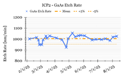
===Process Control: GaAs Etch with N<sub>2</sub>/Cl<sub>2</sub> (Panasonic 2)=== |
|||
[[File:GaAs Etch ICP2 SPC.png|alt=example ICP2 process control chart|thumb|249x249px|[https://docs.google.com/spreadsheets/d/16gHOO3PQn_LinrXGPeSTSBf5dnw3leSLh1gq0PLr43w/edit?gid=1804752281#gid=1804752281 Click for Process Control Charts] for GaAs etching.|link=https://docs.google.com/spreadsheets/d/16gHOO3PQn_LinrXGPeSTSBf5dnw3leSLh1gq0PLr43w/edit?gid=1804752281#gid=1804752281]] |
|||
*[https://docs.google.com/spreadsheets/d/16gHOO3PQn_LinrXGPeSTSBf5dnw3leSLh1gq0PLr43w/edit?gid=0#gid=0 GaAs Etch with N2/Cl2 - '''Etch Data'''] |
|||
*[https://docs.google.com/spreadsheets/d/16gHOO3PQn_LinrXGPeSTSBf5dnw3leSLh1gq0PLr43w/edit?gid=1804752281#gid=1804752281 GaAs Etch with N2/Cl2 - '''Plots'''] |
|||
==Photoresist and ARC etching (Panasonic 2)== |
==Photoresist and ARC etching (Panasonic 2)== |
||
| Line 416: | Line 429: | ||
*[https://wiki.nanotech.ucsb.edu/wiki/images/e/e9/194_Ru_Etch_O2%2CCl2.pdf Ru Etch] - ''[[Bill Mitchell]] 2019-09-19'' |
*[https://wiki.nanotech.ucsb.edu/wiki/images/e/e9/194_Ru_Etch_O2%2CCl2.pdf Ru Etch] - ''[[Bill Mitchell]] 2019-09-19'' |
||
**''This etch is used in the following publication:'' [[Template:Publications#Highly Selective and Vertical Etch of Silicon Dioxide using Ruthenium Films as an Etch Mask|W.J. Mitchell, "Highly Selective and Vertical Etch of Silicon Dioxide using Ruthenium Films as an Etch Mask" (JVST-A, 2021)]] |
**''This etch is used in the following publication:'' [[Template:Publications#Highly Selective and Vertical Etch of Silicon Dioxide using Ruthenium Films as an Etch Mask|W.J. Mitchell, "Highly Selective and Vertical Etch of Silicon Dioxide using Ruthenium Films as an Etch Mask" (JVST-A, 2021)]] |
||
==Process Control Data (Panasonic 2)== |
|||
===GaAs Etch with N<sub>2</sub>/Cl<sub>2</sub> - Process Control Data (Panasonic 2)=== |
|||
*[https://docs.google.com/spreadsheets/d/16gHOO3PQn_LinrXGPeSTSBf5dnw3leSLh1gq0PLr43w/edit?gid=0#gid=0 GaAs Etch with N2/Cl2 - '''Etch Data'''] |
|||
*[https://docs.google.com/spreadsheets/d/16gHOO3PQn_LinrXGPeSTSBf5dnw3leSLh1gq0PLr43w/edit?gid=1804752281#gid=1804752281 GaAs Etch with N2/Cl2 - '''Plots'''][[File:GaAs Etch ICP2 SPC.png|alt=example ICP2 process control chart|none|thumb|249x249px|[https://docs.google.com/spreadsheets/d/16gHOO3PQn_LinrXGPeSTSBf5dnw3leSLh1gq0PLr43w/edit?gid=1804752281#gid=1804752281 Click for Process Control Charts]|link=https://docs.google.com/spreadsheets/d/16gHOO3PQn_LinrXGPeSTSBf5dnw3leSLh1gq0PLr43w/edit?gid=1804752281#gid=1804752281]] |
|||
===SiO<sub>2</sub> Etch with CHF<sub>3</sub>/CF<sub>4</sub> - Process Control Data (Panasonic 2)=== |
|||
*[https://docs.google.com/spreadsheets/d/1m0l_UK2lDxlgww4f6nfXe4aQedNeDZsLs46jQ5wR4zw/edit?usp=sharing SiO2 Etch with CHF3/CF4 - '''Etch Data'''] |
|||
*[https://docs.google.com/spreadsheets/d/1m0l_UK2lDxlgww4f6nfXe4aQedNeDZsLs46jQ5wR4zw/edit#gid=1804752281 SiO2 Etch with CHF3/CF4 - '''Plots'''][[File:ICP2 Process Control Data Example.jpg|alt=example ICP2 process control chart|none|thumb|250x250px|[https://docs.google.com/spreadsheets/d/1m0l_UK2lDxlgww4f6nfXe4aQedNeDZsLs46jQ5wR4zw/edit#gid=1804752281 Click for Process Control Charts]|link=https://docs.google.com/spreadsheets/d/1m0l_UK2lDxlgww4f6nfXe4aQedNeDZsLs46jQ5wR4zw/edit#gid=1804752281]] |
|||
=[[Oxford ICP Etcher (PlasmaPro 100 Cobra)]]= |
=[[Oxford ICP Etcher (PlasmaPro 100 Cobra)]]= |
||
| Line 435: | Line 436: | ||
** The oil fully dissolves in Acetone or NMP. You can clean oil off the back by wiping the back of the sample against an ACE-soaked wipe. |
** The oil fully dissolves in Acetone or NMP. You can clean oil off the back by wiping the back of the sample against an ACE-soaked wipe. |
||
* InP requires fairly high temperatures for making the Indium products volatile - so going to full-wafers (which are cooler) may requiring the table temperature. We have found that temperatures of ~150⁰C minimum may be required for preventing grassing etc. |
* InP requires fairly high temperatures for making the Indium products volatile - so going to full-wafers (which are cooler) may requiring the table temperature. We have found that temperatures of ~150⁰C minimum may be required for preventing grassing etc. |
||
* See the |
* See the '''Process Control sections below''' - [[Process Group Interns|NanoFab Interns]] run Etches Weekly, tracked over time. |
||
** This tells you whether the chamber and tool are operating properly before you run your etch. |
** This tells you whether the chamber and tool are operating properly before you run your etch. |
||
** You can follow the intern's travelers for details of their etch. |
** You can follow the intern's travelers for details of their etch. |
||
==InP Ridge Etch (Oxford ICP Etcher)== |
==InP Ridge Etch (Oxford ICP Etcher)== |
||
===High-Temp (200°C) Process=== |
===High-Temp (200°C) InP Etch Process=== |
||
*InP Ridge Etch 200°C - ''Noah Dutra & Fatt Foong, 2025-08-12'' |
*InP Ridge Etch 200°C - ''Noah Dutra & Fatt Foong, 2025-08-12'' |
||
| Line 447: | Line 448: | ||
**Cal Sample: ~1cm sample etched with 1 quarter of blank 50mm InP seasoning wafer placed '''without''' mounting adhesive on blank Silicon carriers (rough side up). |
**Cal Sample: ~1cm sample etched with 1 quarter of blank 50mm InP seasoning wafer placed '''without''' mounting adhesive on blank Silicon carriers (rough side up). |
||
**Recipe: Cl2/H2/Ar - 200°C |
**Recipe: Cl2/H2/Ar - 200°C |
||
===Low-Temp (60°C) Process=== |
|||
==== Process Control: High-Temp (200°C) InP Etch ==== |
|||
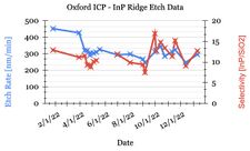
[[File:200C InP.png|alt=example SPC chart for Oxford ICP Etcher|thumb|218x218px|[https://docs.google.com/spreadsheets/d/1LE5Cug9uJFYEwu0ZsNsp0W1dTRzcO2EKFhC0wu3w0n4/edit?gid=1804752281#gid=1804752281 Click for Process Control Charts] for 200°C InP Etch|link=https://docs.google.com/spreadsheets/d/1LE5Cug9uJFYEwu0ZsNsp0W1dTRzcO2EKFhC0wu3w0n4/edit?gid=1804752281#gid=1804752281]]''Calibration / Process testing data taken using the "InP Ridge Etch" process: Cl2/H2/Ar @ 200°C, 1cm piece with ~50% SiO2 hardmask.'' |
|||
*[https://docs.google.com/spreadsheets/d/1LE5Cug9uJFYEwu0ZsNsp0W1dTRzcO2EKFhC0wu3w0n4/edit?gid=0#gid=0 "Std InP Ridge Etch" Cl<sub>2</sub>/H<sub>2</sub>/Ar 200°C - '''Etch Data Tables'''] |
|||
*[https://docs.google.com/spreadsheets/d/1LE5Cug9uJFYEwu0ZsNsp0W1dTRzcO2EKFhC0wu3w0n4/edit?gid=1804752281#gid=1804752281 "Std InP Ridge Etch" Cl<sub>2</sub>/H<sub>2</sub>/Ar 200°C - '''Plots'''] |
|||
===Low-Temp (60°C) InP Etch Process=== |
|||
*[[Media:Oxford Etcher - InP Ridge Etch using Oxford PlasmaPro 100 Cobra - 2021-09-08.pdf|Low-Temp InP Ridge Etch Characterization]] - ''Ning Cao, 2021-09-08'' |
*[[Media:Oxford Etcher - InP Ridge Etch using Oxford PlasmaPro 100 Cobra - 2021-09-08.pdf|Low-Temp InP Ridge Etch Characterization]] - ''Ning Cao, 2021-09-08'' |
||
**<u>''No longer calibrating 60°C process as of 05-2025''.</u> |
**<u>''No longer calibrating 60°C process as of 05-2025''.</u> |
||
| Line 455: | Line 461: | ||
**NOTE: Rates in these 2021-09 characterizations are lower than current due to a software timing bug, fixed in 2022-01 |
**NOTE: Rates in these 2021-09 characterizations are lower than current due to a software timing bug, fixed in 2022-01 |
||
*See [[Oxford ICP Etcher (PlasmaPro 100 Cobra)#Documentation|Operating Procedure]] for full traveler and post-cleaning. |
*See [[Oxford ICP Etcher (PlasmaPro 100 Cobra)#Documentation|Operating Procedure]] for full traveler and post-cleaning. |
||
==== Process Control: Low-Temp (60°C) InP Etch ==== |
|||
[[File:Oxford-ICP-Etch Process Control Data Example.jpg|alt=example SPC chart for Oxford ICP Etcher|thumb|225x225px|[https://docs.google.com/spreadsheets/d/1cEUB7K5BAg9N4vp3rPZw7g0orFkxeQmRkX34Fb4eZco/edit#gid=1804752281 Click for Process Control Charts] for 60°C InP Etch|link=https://docs.google.com/spreadsheets/d/1cEUB7K5BAg9N4vp3rPZw7g0orFkxeQmRkX34Fb4eZco/edit#gid=1804752281]] |
|||
2025-08-12: No longer run as weekly cal process, replaced by above 200°C Cl<sub>2</sub>/H<sub>2</sub>/Ar etch. Data below is for historical purposes only. |
|||
''Calibration / Process testing data taken using the "InP Ridge Etch" process: Cl2/CH4/H2 @ 60°C, 1cm piece with ~50% SiO2 hardmask.'' |
|||
*[https://docs.google.com/spreadsheets/d/1cEUB7K5BAg9N4vp3rPZw7g0orFkxeQmRkX34Fb4eZco/edit?usp=sharing "Std InP Ridge Etch" Cl<sub>2</sub>/CH<sub>4</sub>/H<sub>2</sub>/60°C - '''Etch Data Tables'''] |
|||
*[https://docs.google.com/spreadsheets/d/1cEUB7K5BAg9N4vp3rPZw7g0orFkxeQmRkX34Fb4eZco/edit#gid=1804752281 "Std InP Ridge Etch" Cl<sub>2</sub>/CH<sub>4</sub>/H<sub>2</sub>/60°C - '''Plots'''] |
|||
====[[Oxford Etcher - Sample Size Effect on Etch Rate|Sample Size effect on Etch Rate]]==== |
====[[Oxford Etcher - Sample Size Effect on Etch Rate|Sample Size effect on Etch Rate]]==== |
||
| Line 468: | Line 482: | ||
== GaN Etch (Oxford ICP Etcher) == |
== GaN Etch (Oxford ICP Etcher) == |
||
[[File:Dot Facet 00.jpg|alt=Example SEM image|thumb|170x170px|Example of 1.2um etched GaN, "Dot Facet". (Image Credit: Gopikrishnan Meena 2024-10)]] |
|||
*''[https://drive.google.com/file/d/1B-Xg254T-RdALisnms0jvpJQ34i5TNXN/view?usp=drive_link Std GaN Etch - BCl3/Cl2/Ar - 200C Etch Characterization] - G.G.Meena, 2024-11-01'' |
*''[https://drive.google.com/file/d/1B-Xg254T-RdALisnms0jvpJQ34i5TNXN/view?usp=drive_link Std GaN Etch - BCl3/Cl2/Ar - 200C Etch Characterization] - G.G.Meena, 2024-11-01'' |
||
**Etches characterized on ~1cmx1cm die, on 4<nowiki>''</nowiki> Si carrier wafer. Die has a SiN hard mask. |
**Etches characterized on ~1cmx1cm die, on 4<nowiki>''</nowiki> Si carrier wafer. Die has a SiN hard mask. |
||
| Line 473: | Line 488: | ||
**See [[Oxford ICP Etcher (PlasmaPro 100 Cobra)#Documentation|Operating Procedure]] for full traveler and post-cleaning. |
**See [[Oxford ICP Etcher (PlasmaPro 100 Cobra)#Documentation|Operating Procedure]] for full traveler and post-cleaning. |
||
==== Process Control: GaN Etch ==== |
|||
[[File:GaN SPC.png|alt=example of Process Control Charts|thumb|[https://docs.google.com/spreadsheets/d/1Pk8VwZlZ2lUf3aL9J2El5ZygqHY040TX3ZAMwa33LpE/edit?gid=507237279#gid=507237279 Click for Process Control Charts] for GaN Etch|link=https://docs.google.com/spreadsheets/d/1Pk8VwZlZ2lUf3aL9J2El5ZygqHY040TX3ZAMwa33LpE/edit?gid=507237279#gid=507237279|219x219px]]Recipe: ''Std GaN Etch - BCl3/Cl2/Ar - 200C (Public)'', on 1cm x 1cm ''~1.2µm deep GaN etch with Cl2/BCl3/Ar at 200°C.'' ''GaN-on-Sapphire substrate with SiN mask.'' |
|||
*[https://docs.google.com/spreadsheets/d/1Pk8VwZlZ2lUf3aL9J2El5ZygqHY040TX3ZAMwa33LpE/edit?gid=0#gid=0 GaN Etching with Cl2/BCl3/Ar at 200°C - Etch Data] |
|||
*[https://docs.google.com/spreadsheets/d/1Pk8VwZlZ2lUf3aL9J2El5ZygqHY040TX3ZAMwa33LpE/edit?gid=507237279#gid=507237279 GaN Etching with Cl2/BCl3/Ar at 200°C - Plots] |
|||
==GaAs Etch (Oxford ICP Etcher)== |
==GaAs Etch (Oxford ICP Etcher)== |
||
*''[https://drive.google.com/file/d/1Q4pmX5M9v9dCD1xOg74kYguV12Szh9be/view?usp=drive_link Std GaAs Etch - BCl3/Ar - 20C Etch Characterization] - G.G.Meena, 2025-01-09'' |
*''[https://drive.google.com/file/d/1Q4pmX5M9v9dCD1xOg74kYguV12Szh9be/view?usp=drive_link Std GaAs Etch - BCl3/Ar - 20C Etch Characterization] - G.G.Meena, 2025-01-09'' |
||
| Line 484: | Line 503: | ||
==Cleaning Recipes (Oxford ICP Etcher)== |
==Cleaning Recipes (Oxford ICP Etcher)== |
||
'''''To Be Added: Required cleaning time & recipes''''' |
'''''To Be Added: Required cleaning time & recipes''''' |
||
==Process Control Data (Oxford ICP Etcher)== |
|||
===[https://docs.google.com/spreadsheets/d/1LE5Cug9uJFYEwu0ZsNsp0W1dTRzcO2EKFhC0wu3w0n4/edit?gid=0#gid=0 NEW Process Control Data for "Std InP Ridge Etch" Cl<sub>2</sub>/H<sub>2</sub>/Ar/200°C]=== |
|||
''Calibration / Process testing data taken using the "InP Ridge Etch" process: Cl2/H2/Ar @ 200°C, 1cm piece with ~50% SiO2 hardmask.'' |
|||
*[https://docs.google.com/spreadsheets/d/1LE5Cug9uJFYEwu0ZsNsp0W1dTRzcO2EKFhC0wu3w0n4/edit?gid=0#gid=0 "Std InP Ridge Etch" Cl<sub>2</sub>/H<sub>2</sub>/Ar 200°C - '''Etch Data Tables'''] |
|||
*[https://docs.google.com/spreadsheets/d/1LE5Cug9uJFYEwu0ZsNsp0W1dTRzcO2EKFhC0wu3w0n4/edit?gid=1804752281#gid=1804752281 "Std InP Ridge Etch" Cl<sub>2</sub>/H<sub>2</sub>/Ar 200°C - '''Plots'''][[File:200C InP.png|alt=example SPC chart for Oxford ICP Etcher|none|thumb|344x344px|[https://docs.google.com/spreadsheets/d/1LE5Cug9uJFYEwu0ZsNsp0W1dTRzcO2EKFhC0wu3w0n4/edit?gid=1804752281#gid=1804752281 Click for Process Control Charts]|link=https://docs.google.com/spreadsheets/d/1LE5Cug9uJFYEwu0ZsNsp0W1dTRzcO2EKFhC0wu3w0n4/edit?gid=1804752281#gid=1804752281]] |
|||
===[https://docs.google.com/spreadsheets/d/1cEUB7K5BAg9N4vp3rPZw7g0orFkxeQmRkX34Fb4eZco/edit#gid=1804752281 OLD Process Control Data for "Std InP Ridge Etch" Cl<sub>2</sub>/CH<sub>4</sub>/H<sub>2</sub>/60°C]=== |
|||
2025-08-12: No longer run as weekly cal process, replaced by above 200°C Cl<sub>2</sub>/H<sub>2</sub>/Ar etch. Data below is for historical purposes only. |
|||
''Calibration / Process testing data taken using the "InP Ridge Etch" process: Cl2/CH4/H2 @ 60°C, 1cm piece with ~50% SiO2 hardmask.'' |
|||
*[https://docs.google.com/spreadsheets/d/1cEUB7K5BAg9N4vp3rPZw7g0orFkxeQmRkX34Fb4eZco/edit?usp=sharing "Std InP Ridge Etch" Cl<sub>2</sub>/CH<sub>4</sub>/H<sub>2</sub>/60°C - '''Etch Data Tables'''] |
|||
*[https://docs.google.com/spreadsheets/d/1cEUB7K5BAg9N4vp3rPZw7g0orFkxeQmRkX34Fb4eZco/edit#gid=1804752281 "Std InP Ridge Etch" Cl<sub>2</sub>/CH<sub>4</sub>/H<sub>2</sub>/60°C - '''Plots'''][[File:Oxford-ICP-Etch Process Control Data Example.jpg|alt=example SPC chart for Oxford ICP Etcher|none|thumb|225x225px|[https://docs.google.com/spreadsheets/d/1cEUB7K5BAg9N4vp3rPZw7g0orFkxeQmRkX34Fb4eZco/edit#gid=1804752281 Click for Process Control Charts]|link=https://docs.google.com/spreadsheets/d/1cEUB7K5BAg9N4vp3rPZw7g0orFkxeQmRkX34Fb4eZco/edit#gid=1804752281]] |
|||
=== [https://docs.google.com/spreadsheets/d/1Pk8VwZlZ2lUf3aL9J2El5ZygqHY040TX3ZAMwa33LpE/edit?gid=0#gid=0 Process Control Data for "GaN Etch" (Cl2/BCl3/Ar/200°C)] === |
|||
[[File:Dot Facet 00.jpg|alt=Example SEM image|thumb|170x170px|Example of 1.2um etched GaN, "Dot Facet". (Image Credit: Gopikrishnan Meena 2024-10)]]Recipe: ''Std GaN Etch - BCl3/Cl2/Ar - 200C (Public)'', on 1cm x 1cm ''~1.2µm deep GaN etch with Cl2/BCl3/Ar at 200°C.'' Sapphire substrate with SiN mask for GaN. |
|||
*[https://docs.google.com/spreadsheets/d/1Pk8VwZlZ2lUf3aL9J2El5ZygqHY040TX3ZAMwa33LpE/edit?gid=0#gid=0 GaN Etching with Cl2/BCl3/Ar at 200°C - Etch Data] |
|||
*[https://docs.google.com/spreadsheets/d/1Pk8VwZlZ2lUf3aL9J2El5ZygqHY040TX3ZAMwa33LpE/edit?gid=507237279#gid=507237279 GaN Etching with Cl2/BCl3/Ar at 200°C - Plots][[File:GaN SPC.png|alt=example of Process Control Charts|none|thumb|[https://docs.google.com/spreadsheets/d/1Pk8VwZlZ2lUf3aL9J2El5ZygqHY040TX3ZAMwa33LpE/edit?gid=507237279#gid=507237279 Click for Process Control Charts]|link=https://docs.google.com/spreadsheets/d/1Pk8VwZlZ2lUf3aL9J2El5ZygqHY040TX3ZAMwa33LpE/edit?gid=507237279#gid=507237279]] |
|||
Latest revision as of 00:02, 20 November 2025
Back to Dry Etching Recipes.
DSEIII_(PlasmaTherm/Deep_Silicon_Etcher)
Process Tips
- Use the Santovac oil for mounting small pieces to Silicon carrier wafers, or else your resist will burn! Increases thermal conduction to the cooled carrier wafer. (Full-wafers instead get direct Helium cooling.) Careful that the oil does not get anywhere near the outer clamp that holds the wafer down, or your wafer will get stuck.
- The oil fully dissolves in Acetone or NMP. You can clean oil off the back by wiping the back of the sample against an ACE-soaked wipe.
- See the Process Control Data below - Staff/Intern-run Etches Weekly, tracked over time.
- This tells you whether the chamber and tool are operating properly before you run your etch.
- You can follow the intern's travelers for details of their etch.
Edge-Bead Removal (DSEiii)
Make sure to remove photoresist from edges of wafer, or PR may stick to the top-side wafer clamp and destroy your wafer during unload!
- Edge Bead Removal via Photolithography: use a custom metal mask to pattern the photoresist with a flood exposure.
- If you are etching fully through a wafer, remember that removal of edge-bead will cause full etching in the exposed areas. To prevent a wafer from falling into the machine after the etch, you can mount to a carrier wafer using wax.
- Manual PR Edge-Bead Removal - using swabs and EBR100. This is prone to error and easy to accidentally leave a blob of PR on the edge - so be extra careful to ensure NO PR is left on the edges!
High Rate Bosch Etch (DSEIII)
- Bosch Process Recipe and Characterization - Standard recipe on the tool.
Example of 100µm Deep Bosch Etched Silicon posts with Al2O3 hard mask. Close inspection shows the horizontal "scalloping" from the cycling nature of the etch. (Image Credit: Demis D. John, 2021-07) - STD_Bosch_Si (⭐️Production) - Developed 2024-10
- Old Recipe Name: "Plasma-Therm Standard DSE" - lower EtchA, less tolerant
- Standard Bosch Process for high aspect-ratio, high-selectivity Silicon etching.
- Cycles between polymer deposition "Dep" / Polymer etch "Etch A" / Si etch "Etch B" steps. Step Times gives fine control.
- To reduce roughening/grassing ("black silicon"), Increase "Etch A" time by ~50%. Alternatively, reduce "Dep" step time by ~20%.
- Patterns with different exposed/etched areas will have different "optimal" parameters.
- This recipe has 2s Etch A time compared to "Plasma-Therm Standard DSE" (which has 1.5s Etch A) below - this reduced the undercut of mask to ~1% of the etch depth and the effect of aspect ratio on etch rate. All other recipe parameters are the same.
- Selectivity to Photoresist ~60.
- Selectivity to SiO2 should be higher, not yet measured.
- Selectivity to Al2O3 is extremely high, >9000. See below TSV process for processing tips with Al2O3 hardmask.
- If you need to pattern all the way to the edge of the wafer, PR won't work because you have to remove the edge-bead of photoresist (see above). Instead use hardmask process (See "Through Silicon Via" etch below).
- <1% center to edge variability in etch rate.
- Larger open area → lower selectivity & lower etch rate.
- Thick PR's approx ≥10µm tend to burn, avoid thick PR's. They also make edge-bead removal very difficult. Instead use an SiO2 hardmask or the Al2O3/SiO2 hardmask below.
- STD_Bosch_Si (⭐️Production) - Developed 2024-10

 |
 |
Si Etching C4F8/SF6/Ar (PlasmaTherm DSEiii)
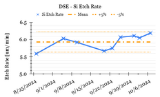
- Recipe: STD_Bosch_Si (⭐️Production), on 100mm Si Wafer with ~50% open area, photoresist mask, ~40µm deep
Through Silicon Via (TSV) etch (DSEiii)
Since the topside clamp requires the removal of photoresist on the outermost ~5-7mm of the wafer, this makes PR incompatible with through-silicon etching (as the outer edges would be etched-through, dropping the inner portion into the chamber). In addition, in practice we have found that thick PR often roughens and burns during long ~30-60min etches, making removal very difficult.
Instead, we recommend the following process with Al2O3 hardmask:
NOTE: We have recently found that the wax-mounting process process can leave wax on the wafer clamp, causing the next user's wafer to get stuck and fail transfer!  DO NOT RUN the wax-mounting process without discussing with staff first. (Through-wafer process with no wax is still acceptable.) -- Demis 2024-03-11

Staff is working on a dicing-tape mounted recipe, to be published here soon.
-- Demis 2025-11-19
| Process for Through-Wafer Silicon Etching | |
|---|---|
| Process to etch through ~550µm Silicon | Demis D. John & Biljana Stamenic 2022-11-11. Please consider our publication policy if you use/modify this process. |
Deposit 150nm Al2O3 on either:
|
May need to do dep. rate check beforehand. |
| Deposit ~3nm SiO2, in situ (same machine as above) | This improves adhesion to photoresist and prevents developer attacking the Al2O3. |
| Lithography - your preferred method. Needs approx. ≥500nm thick PR. | |
| Etch the Al2O3 in Panasonic ICP 1/2 | Use 50W version. Overetch by ~20%, will also etch through the thin SiO2 layer. |
| Strip PR - either in situ, or via NMP 80°C soak followed by PEii Technics ashing. | In situ PR strip appears to give better + faster results. |
| If pieces of the wafer are at risk of falling into the chamber, mount the product wafer to a carrier wafer:
Logitech Wax Mounting Recipe - Bulk Crystal Bond
|
CONTACT STAFF before attempting this step!
|
| Use POLOS spinners with ACE/ISO to clean front and back of wafer.
IMPORTANT for wax-mounting, to ensure wax does not stick your wafer to the DSE clamp. Observe carefully for any wax protruding from between wafers - redo spin-clean as needed. |
Also make sure wax thickness is not too thick, of long etches could cause wax to seep out from between the wafers. |
DSEiii etch - reduce Dep step to eliminate grassing:
|
Can use Lasermonitor and/or Camera to observe when etch is fully through. Trenches may get black/rough, but then clear up when fully etched.
|
| If you did not wax-mount your wafer, the recipe will eventually fail for Helium Pressure/Flow out of compliance. This is because the cooling Helium leaks through the wafer when the openings get fully etched through.
Once this happens,
|
|
| Strip Al2O3/SiO2 either with Buffered HF, or same Pan1/2 dry etch as above.
BHF: Eg. ~2min to fully remove SiO2 + Al2O3, with overetch. |
See etch BHF rates of the thin-films on this table. |
IF wax-mounted - either
OR
|
|
| If you publish using the above process, please consider our publication policy. This process was developed by Biljana Stamenic and Demis D. John, 2022. | |
Single-Step Low Etch Rate Smooth Sidewall Process (DSEIII)
- Single Step Silicon Etch Recipe and Characterization
- Recipe Name: "Nano Trench Etch" (Production - copy to your Personal category)
- Used instead of Bosch Process, to avoid scalloping on the sidewall.
- Lower selectivity, lower etch rate, smoother sidewalls.
PlasmaTherm/SLR Fluorine Etcher
Process Tips
- Use the Santovac oil for mounting small pieces to Silicon carrier wafers, or else your resist will burn! Increases thermal conduction to the cooled carrier wafer. (Full-wafers instead get direct Helium cooling.) Careful that the oil does not get anywhere near the outer clamp that holds the wafer down, or your wafer will get stuck.
- The oil fully dissolves in Acetone or NMP. You can clean oil off the back by wiping the back of the sample against an ACE-soaked wipe.
- See the Process Control Data below - Staff/Intern-run Etches Weekly, tracked over time.
- This tells you whether the chamber and tool are operating properly before you run your etch.
- You can follow the intern's travelers for details of their etch.
Recipe Tips
- RF1: Bias Power (with DCV readback)
- RF2: ICP Power
- For trouble igniting ICP plasma, add 15 to 75 W of bias power during ignition step. Typical ignition pressures 5 to 10 mT.
Si Etch Recipes (Fluorine ICP Etcher)
.jpg)
- "SiVertHFv2" (⭐️Production)
- 20mTorr, RF=18W, ICP=950W, C4F8/SF6/CF4=120/48/54sccm
- This recipe has 2x gas flow compared to "SiVertHF" below - this reduced the loading effect (dependence on % etched area).
- Selectivity Silicon:Photoresist ≈ 5
- Etch Rates: Si ≈ 300-350 nm/min; SiO2 ≈ 30-35 nm/min
- 89-90 degree etch angle, ie, vertical.
- High selectivity to Al2O3 masks.
- Process Control Data above - Staff/Intern-run Etches Weekly, tracked over time.
- 20mTorr, RF=18W, ICP=950W, C4F8/SF6/CF4=120/48/54sccm
- Old Recipe: SiVertHF - Si Vertical Etch using C4F8/SF6/CF4 and resist mask
Process Notes/Observations
- Due to high selectivity against SiO2, it may be necessary to run a ~10sec 50W SiO2 etch (below) to remove native oxide on Si. This can be performed in situ before the Si etch. It's possible this is actually an effect of photoresist open-area - we have conflicting results.
- If you see very low etch rates, try the above SiO2 etch, or try a short PR/BARC etch.
- We have observed that full-wafers with small open area in photoresist masks might require a recalibration of the C4F8/SF6 ratio in order to prevent very low etch rates.
Process Control: Si Etching C4F8/SF6/CF4 (Fluorine ICP Etcher)
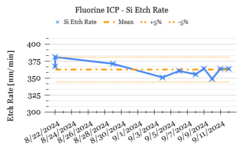
Full Wafer Si etching with ~50% open area and resist mask, run weekly by NanoFab Interns.
SiO2 Etch Recipes (Fluorine ICP Etcher)


- "SiO2 Etch-50W" (⭐️Production)
- 3.8mT, RF=50W, ICP=900W, CHF3/CF4=10/30sccm
- SiO2 etch rate: ~250nm/min
- Selectivity SiO2:Photoresist ≈ 1.10–1.20
- Selectivity SiO2:Ru ≈ 36
- Process Control Data Above - Staff/Intern-run Etches Weekly, tracked over time.
SiO2 Etching using Ruthenium Hardmask
- Click above for Full Process Traveler
- Process written for Sputtered Ru & I-Line GCA Stepper litho
- Can be transferred to ALD Ru or DUV/EBL Litho.
- Ning Cao & Bill Mitchell, 2019-06
- High-selectivity and deep etching using sputtered Ru hardmask and I-Line litho.
- Etch also works well with PR masking
- Chemistry: CHF3/CF4
- Variations in SiO2 etch Bias Power: 50 / 200 / 400W bias.
- Ru etch selectivity to PR: 0.18 (less than 1): 150nm Ru / 800nm PR
- 50W Bias: (recommended)
- Selectivity to photoresist: 1.10–1.20
- SiO2 selectivity to Ru: 36
- SiO2 etch rate: 263nm/min
- Smoothest vertical etch for SiO2.
- 200W Bias: (higher etch rate)
- SiO2 selectivity to Ru: 38
- SiO2 etch rate: 471nm/min
- This etch is detailed in the following article: W.J. Mitchell et al., JVST-A, May 2021
- Updates: Many users have found that SiO2-masking the Ru hardmask results in vastly improved photoresist selectivity, making litho+etch of small features much better.
- Layer stack looks like: SiO2 (or other dielectric target layer to etch) / Ru hardmask / SiO2 hardmask (thin) / Photoresist.
- Typically strip the masks+PR with all dry etching. That means the entire etch process (all etches and strips) can be run in situ on the Panasonic ICP in a rapid single-tool etch process.
Process Control: SiO2 Etching with CHF3/CF4 (Fluorine ICP Etcher)
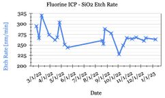
Full Wafer Si etching with ~50% open area and resist mask, run weekly by NanoFab Interns.
Si3N4 Etching (Fluorine ICP Etcher)
Developed by Bill Mitchell. Please see publication policy.
- ICP = 950/75W
- Pressure = 5mT
- Low Polymer Dep: CF4 = 60sccm
- Etch Rate = 420nm/min (PECVD Si3N4)
- Higher verticality: CF4 = 35 / CHF3 = 25 sccm
- Etch Rate = 380nm/min (PECVD Si3N4)
Photoresist & ARC (Fluorine ICP Etcher)
Chain multiple Recipes in a Flow, to allow you to to do in situ BARC etching, and follow up with in situ Photoresist Strip.
PR/BARC Etch (Fluorine ICP Etcher)
- Etching DUV42P-6 Bottom Anti-Reflection Coating
- ~60nm thick (2500krpm)
- O2=20sccm / 10mT / RF1(bias)=100W / RF2(icp)=0W
- 45sec-1min

Photoresist Strip/Polymer Removal (Fluorine ICP Etcher)
Old PR strip recipe: PostBARC Etch/PR Strip (STD)
- O2=100sccm / 5mT / RF1(bias)=10W / RF2(icp)=825W
- 75W Bias can be helpful for difficult to remove polymers, eg. 2min
- Use laser monitor to check for complete removal, overetch to remove Fluorocarbon polymers.
- Not able to completely remove PR (both negative & positive) after prolonged over etching (over etching of +2min)
- Leaves behind residue on the sides

New PR strip recipe: PostBARC Etch/PR Strip (STD)_V2
- O2=100sccm / 5mT / RF1(bias)=100W / RF2(icp)=825W
- RF bias increased by 10x to 100W
- Able to completely remove PR (both negative & positive) after over etching (over etching of +2min)
- Clean surface with no residue
Cleaning Procedures (Fluorine ICP Etcher)
To Be Added
ICP Etch 1 (Panasonic E646V)
Panasonic ICP#1 is currently down - Use Panasonic ICP#2 instead. Most processes directly transfer with only small change in etch rate. Data kept here for historical purposes only.
SiO2 Etching (Panasonic 1)
Recipes
- SiO2 Vertical Etch Recipe Parameters - CHF3 "SiOVert"
- Etch rate ≈ 2300Å/min (users must calibrate)
- Selectivity (SiO2:Photoresist) ≈ greater than 1:1 (users must calibrate)
Recipe Variations
Use these to determine how each etch parameter affects the process.
- SiO2 CHF3 Etch Variations - CHF3 with varying Bias and Pressure, Slanted SiO2 etching
SiNx Etching (Panasonic 1)
Al Etch (Panasonic 1)
Cr Etch (Panasonic 1)
Ta Etch (Panasonic 1)
- Ta Etch Recipe - Cl2/BCl3
Ti Etch (Panasonic 1)
W-TiW Etch (Panasonic 1)
GaAs-AlGaAs Etch (Panasonic 1)
- GaAs-Nanoscale Etch Recipe - PR mask - Cl2-BCl3-Ar
- AlGaAs Etch Recipes - Cl2N2
- GaAs DRIE via Etch Recipes - Cl2-BCl3-Ar PR passivation
GaN Etch (Panasonic 1)
Photoresist and ARC Etching (Panasonic 1)
Please see the recipes for Panasonic ICP#2 - the same recipes apply.
Etching of DUV42P at standard spin/bake parameters also completes in 45 seconds.
SiC Etch (Panasonic 1)
Sapphire Etch (Panasonic 1)
Cleaning Recipes
To Be Added
Old Deleted Recipes
Since there are a limited number of recipe slots on the tool, we occasionally have to delete old, unused recipes.
If you need to free up a recipe slot, please contact the tool's Supervisor and they'll help you find an old recipe to replace. We take photographs of old recipes, and save them in case a group needs to revive the recipe. Contact us if your old recipe went missing.
Process Control Data (Panasonic 1)
SiO2 Etch with CHF3/CF4 - Process Control Data (Panasonic 1)
ICP Etch 2 (Panasonic E626I)
Recipes starting points for materials without processes listed can be obtained from Panasonic1 recipe files. The chambers are slightly different, but essentially the same, requiring only small program changes to obtain similar results.
Process Tips
- Use the Santovac oil for mounting small pieces to Silicon carrier wafers, or else your resist will burn! Increases thermal conduction to the cooled carrier wafer. (Full-wafers instead get direct Helium cooling.) Careful that the oil does not get on the back of the carrier wafer or you will get Helium cooling errors.
- The oil fully dissolves in Acetone or NMP. You can clean oil off the back by wiping the back of the sample against an ACE-soaked wipe.
- See the Process Control sections below - NanoFab Interns run Etches Weekly, tracked over time.
- This tells you whether the chamber and tool are operating properly before you run your etch.
- You can follow the intern's travelers for details of their etch, and see their SEM's.
SiO2 Etching (Panasonic 2)
Recipes
- SiO2 Vertical Etch Recipe#2 - CF4/CHF3
- This etch is used in our Process Control weekly cals run by NanoFab Interns. Very stable over time ±5%.
- SiO2 Nanoscale Etch Recipe - CHF3/O2
- SiO2 Vertical Etch Recipe - CHF3 "SiOVert"
- Direct copy of "SiOVert" from ICP#1, see parameters there.
Recipe Variations
Use these to determine how etch parameters affect the process.
Process Control: SiO2 Etch with CHF3/CF4 (Panasonic 2)

Weekly cal etches of the CF4/CHF3 SiO2 etch, run by NanoFab Interns.
SiNx Etching (Panasonic 2)
Al Etch (Panasonic 2)
Al2O3 Etching (Panasonic 2)
ALD Al2O3 Etch Rates in BCl3 Chemistry (click for plots of etch rate)
Contributed by Brian Markman, 2018
- BCl3 = 30sccm
- Pressure = 0.50 Pa
- ICP Source RF = 500
- Bias RF = 50W or 250W (250W can burn PR)
- Cooling He Flow/Pressure = 15.0 sccm / 400 Pa
- Etch Rate 50W: 39.6nm/min (0.66nm/sec)
- Etch Rate 250W: 60.0nm/min (1.0 nm/sec)
GaAs Etch (Panasonic 2)
- GaAs Etch Cal - Noah Dutra & Fatt Foong, 2025-02-12
- Etch Rates ~1um/min, Selectivity to SiO2 ~ 27:1, Sidewalls ~ 90°
- Etch Rate/Selectivity highly sensitive to pressure (image credit: Terry Guerrero)
- Cal Sample: ~1cm sample etched mounted with oil onto 150mm Si carrier
- Recipe: 0.5Pa, 100/900W, N2/Cl2=10/20sccm
- Non-Calibration GaAs Etch Recipes - Panasonic 2 - Cl2N2
Process Control: GaAs Etch with N2/Cl2 (Panasonic 2)
Photoresist and ARC etching (Panasonic 2)
Basic recipes for etching photoresist and Bottom Anti-Reflection Coating (BARC) underlayers are as follows:
ARC Etching: DUV-42P or AR6 (Panasonic 2)
- O2 = 40 sccm // 0.5 Pa
- ICP = 75W // RF = 75W
- 45 sec for full etching (incl. overetch) of ~60nm DUV-42P (same as for AR6; 2018-2019, Demis/BrianT)
Photoresist Etch/Strip (Panasonic 2)
Works very well for photoresist stripping
- O2 = 40 sccm // 1.0 Pa
- ICP = 350W // RF = 100W
- Etch Rate for UV6-0.8 (DUV PR) = 518.5nm / 1min (2019, Demis)
- 2m30sec to fully remove UV6-0.8 with ~200% overetch (2019, Demis)
Ru (Ruthenium) Etch (Panasonic 2)
- Ru Etch - Bill Mitchell 2019-09-19
- This etch is used in the following publication: W.J. Mitchell, "Highly Selective and Vertical Etch of Silicon Dioxide using Ruthenium Films as an Etch Mask" (JVST-A, 2021)
Oxford ICP Etcher (PlasmaPro 100 Cobra)
Process Tips
- Use the Santovac oil for mounting small pieces to Silicon carrier wafers, or else your resist will burn! Increases thermal conduction to the cooled carrier wafer. (Full-wafers instead get direct Helium cooling.) Careful that the oil does not get anywhere near the outer clamp that holds the wafer down, or your wafer will get stuck.
- The oil fully dissolves in Acetone or NMP. You can clean oil off the back by wiping the back of the sample against an ACE-soaked wipe.
- InP requires fairly high temperatures for making the Indium products volatile - so going to full-wafers (which are cooler) may requiring the table temperature. We have found that temperatures of ~150⁰C minimum may be required for preventing grassing etc.
- See the Process Control sections below - NanoFab Interns run Etches Weekly, tracked over time.
- This tells you whether the chamber and tool are operating properly before you run your etch.
- You can follow the intern's travelers for details of their etch.
InP Ridge Etch (Oxford ICP Etcher)
High-Temp (200°C) InP Etch Process
- InP Ridge Etch 200°C - Noah Dutra & Fatt Foong, 2025-08-12
- Etch rates ~2 um/min, Selectivity to SiO2 ~ 30:1, Sidewalls ~90°
- Very dependent on open area, more area => lower E.R.s
- Cal Sample: ~1cm sample etched with 1 quarter of blank 50mm InP seasoning wafer placed without mounting adhesive on blank Silicon carriers (rough side up).
- Recipe: Cl2/H2/Ar - 200°C
Process Control: High-Temp (200°C) InP Etch
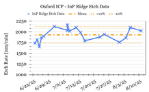
Calibration / Process testing data taken using the "InP Ridge Etch" process: Cl2/H2/Ar @ 200°C, 1cm piece with ~50% SiO2 hardmask.
- "Std InP Ridge Etch" Cl2/H2/Ar 200°C - Etch Data Tables
- "Std InP Ridge Etch" Cl2/H2/Ar 200°C - Plots
Low-Temp (60°C) InP Etch Process
- Low-Temp InP Ridge Etch Characterization - Ning Cao, 2021-09-08
- No longer calibrating 60°C process as of 05-2025.
- InP etches were characterized with no mounting adhesive used, 1/4-wafer of 50mm wafer placed on blank Silicon carriers (rough side up).
- Recipe: Cl2/CH4/H2 - 60°C
- NOTE: Rates in these 2021-09 characterizations are lower than current due to a software timing bug, fixed in 2022-01
- See Operating Procedure for full traveler and post-cleaning.
Process Control: Low-Temp (60°C) InP Etch
2025-08-12: No longer run as weekly cal process, replaced by above 200°C Cl2/H2/Ar etch. Data below is for historical purposes only.
Calibration / Process testing data taken using the "InP Ridge Etch" process: Cl2/CH4/H2 @ 60°C, 1cm piece with ~50% SiO2 hardmask.
- "Std InP Ridge Etch" Cl2/CH4/H2/60°C - Etch Data Tables
- "Std InP Ridge Etch" Cl2/CH4/H2/60°C - Plots
Sample Size effect on Etch Rate
See the above table for data showing effect on sample size/exposed etched area.
InP Grating Etch (Oxford ICP Etcher)
- InP/InGaAsP Grating Etch Characterization - Ning Cao, 2021-08-26
- InP/InGaAsP etches were characterized with no mounting adhesive used, 1/4-wafer of 50mm wafer placed on Silicon carriers (rough side up).
- Recipe: Cl2/CH4/H2/Ar - 20°C
- NOTE: Rates in these 2021-09 characterizations are lower than current due to a software timing bug, fixed in 2022-01
- See Operating Procedure for full traveler and post-cleaning.
GaN Etch (Oxford ICP Etcher)

- Std GaN Etch - BCl3/Cl2/Ar - 200C Etch Characterization - G.G.Meena, 2024-11-01
- Etches characterized on ~1cmx1cm die, on 4'' Si carrier wafer. Die has a SiN hard mask.
- Etch development traveler with detailed characterization data
- See Operating Procedure for full traveler and post-cleaning.
Process Control: GaN Etch
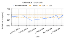
Recipe: Std GaN Etch - BCl3/Cl2/Ar - 200C (Public), on 1cm x 1cm ~1.2µm deep GaN etch with Cl2/BCl3/Ar at 200°C. GaN-on-Sapphire substrate with SiN mask.
GaAs Etch (Oxford ICP Etcher)
- Std GaAs Etch - BCl3/Ar - 20C Etch Characterization - G.G.Meena, 2025-01-09
- Etch characterization on 1cmx1cm die, on 4'' Si carrier wafer. Die has SiO hard mask
- Also tested etch with PR mask.
- See Operating Procedure for full traveler and post-cleaning
GaN Atomic Layer Etching (Oxford ICP Etcher)
GaN-ALE Recipe written and tested by users - contact supervisor for use.
Cleaning Recipes (Oxford ICP Etcher)
To Be Added: Required cleaning time & recipes