RIE 5 (PlasmaTherm): Difference between revisions
No edit summary |
|||
| Line 14: | Line 14: | ||
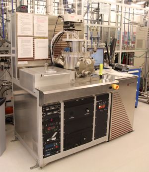
This computer-controlled, turbo-pumped RIE is the "work horse" of the processing laboratory due to it's ease of operation and versatility. It can be operated manually or in a fully programmable mode from sample loading to etching to sample unloading. Samples are placed on a silicon carrier with or without a bonding agent to facilitate sample cooling. Etching is done with oxygen or chlorine-based gases @ 13.56 Mhz. Oxygen is used for etching of photoresists and polyimide. Chlorine-based gases are used for etching semiconductors and some metals. Typical semiconductor materials that are etched are: AlGaAs, InGaAs, AlGaSb, GaN, and Si. Metals that can be etched include Al, Ti, and thin Pt layers. Good masking materials for the chlorine-based etching are photoresist (at powers < 200 W), Ni, SiO<sub>2</sub>, and SrF<sub>2</sub>. The wafer chuck can be heated to 80°C through liquid-based heating. This makes etching of high In-containing compounds difficult due to the non-volatility of In-chlorides. A high physical component (Ar in the mixture) is required for etching of InP and the surface will be contaminated with residual etch products when finished. |
This computer-controlled, turbo-pumped RIE is the "work horse" of the processing laboratory due to it's ease of operation and versatility. It can be operated manually or in a fully programmable mode from sample loading to etching to sample unloading. Samples are placed on a silicon carrier with or without a bonding agent to facilitate sample cooling. Etching is done with oxygen or chlorine-based gases @ 13.56 Mhz. Oxygen is used for etching of photoresists and polyimide. Chlorine-based gases are used for etching semiconductors and some metals. Typical semiconductor materials that are etched are: AlGaAs, InGaAs, AlGaSb, GaN, and Si. Metals that can be etched include Al, Ti, and thin Pt layers. Good masking materials for the chlorine-based etching are photoresist (at powers < 200 W), Ni, SiO<sub>2</sub>, and SrF<sub>2</sub>. The wafer chuck can be heated to 80°C through liquid-based heating. This makes etching of high In-containing compounds difficult due to the non-volatility of In-chlorides. A high physical component (Ar in the mixture) is required for etching of InP and the surface will be contaminated with residual etch products when finished. |
||
Special features include: a true sample loadlock, substrate backside helium cooling, heating up to 80°C, four inch sample holder, HeNe laser etch monitor and chart recorder. Various devices that use this tool as an integral processing step include: in-plane lasers, VCSELs, micro-lenses, Bragg-Fresnel lens, FETs, HBTs, etc. |
Special features include: a true sample loadlock, substrate backside helium cooling, heating up to 80°C, four inch sample holder, HeNe laser etch monitor and chart recorder. Various devices that use this tool as an integral processing step include: in-plane lasers, VCSELs, micro-lenses, Bragg-Fresnel lens, FETs, HBTs, etc. |
||
= Docmentation = |
|||
= Detailed Specifications = |
= Detailed Specifications = |
||
Revision as of 17:15, 17 April 2014
| |||||||||||||||||||||
About
This computer-controlled, turbo-pumped RIE is the "work horse" of the processing laboratory due to it's ease of operation and versatility. It can be operated manually or in a fully programmable mode from sample loading to etching to sample unloading. Samples are placed on a silicon carrier with or without a bonding agent to facilitate sample cooling. Etching is done with oxygen or chlorine-based gases @ 13.56 Mhz. Oxygen is used for etching of photoresists and polyimide. Chlorine-based gases are used for etching semiconductors and some metals. Typical semiconductor materials that are etched are: AlGaAs, InGaAs, AlGaSb, GaN, and Si. Metals that can be etched include Al, Ti, and thin Pt layers. Good masking materials for the chlorine-based etching are photoresist (at powers < 200 W), Ni, SiO2, and SrF2. The wafer chuck can be heated to 80°C through liquid-based heating. This makes etching of high In-containing compounds difficult due to the non-volatility of In-chlorides. A high physical component (Ar in the mixture) is required for etching of InP and the surface will be contaminated with residual etch products when finished.
Special features include: a true sample loadlock, substrate backside helium cooling, heating up to 80°C, four inch sample holder, HeNe laser etch monitor and chart recorder. Various devices that use this tool as an integral processing step include: in-plane lasers, VCSELs, micro-lenses, Bragg-Fresnel lens, FETs, HBTs, etc.
Docmentation
Detailed Specifications
- Etch gases include: Cl2, BCl3, SiCl4, O2, Ar
- Full computer control or manual computer control
- Low 1 E-7 ultimate chamber pressure
- 13.56 Mhz excitation frequency
- Sample chuck He-backside cooled / heated (up to 80°C)
- Typical etch conditions for GaAs:
- 10 mT (15 sccm BCl3 / 10 sccm SiCl4)
- 100 W, constant power
- 60 nm / min. etch rate
