News from the U.C. Santa Barbara Nanofabrication Facility.
ProtoFab Opening Summer 2026
The Nanofab is launching a Prototyping Facility called the "Protofab", which is located at UCSB's new OASIS building. Learn more at https://protofab.oasis.ucsb.edu
The new lab will enable taking your diced chips from the Nanofab, to the Protofab where you can wirebond, attach to PCB's/carriers, align+attach optical fibers etc., to make a real "prototype". The lab is expected to open in Summer 2026, with equipment currently being installed.
Access & model is similar to the Nanofab - anyone can pay an hourly fee to go into the Protofab, using key fobs for access. (OASIS "Membership" is not required to use the Protofab, unless you also want your own desk + private lab space at OASIS.)
Contact the Protofab lab manager Arin Abed for more information.
// Demis D. John 19:51, 27 May 2026 (UTC)
DREAMS Hub awarded 2 projects in GaN and 5G/6G technologies
CA DREAMS Hub is awarded $31.9 million in funding under the Microelectronics Commons -
- $16.2 Million to develop advanced gallium nitride (GaN) semiconductor technologies, with partners including USC, Northrop Grumman, Teledyne Technologies, HRL Laboratories, PseudolithIC, Monde Wireless Inc., Transphorm, UCLA and UC Santa Barbara.
- $15.7 Million in Funding for 5G/6G millimeter-wave Phased-Array Prototypes, with team USC, Northrop Grumman, HRL Laboratories, Teledyne, Caltech, UCLA, UC Santa Barbara, UC San Diego, Vorago, Global Foundries.
// Demis D. John 16:32, 23 September 2024 (PDT)
NSF-ATE Award for SBCC and UCSB: New Semiconductor Pathway
The UCSB NanoFab and CNSI were recently awarded a project by NSF-ATE to build a semiconductor pathway (associates degree or certificate) at Santa Barbara City College, utilizing UCSB Cleanrooms. The project "Expansion of CCPRIME: Central Coast Partnership for Regional Industry-Focused Micro/Nanotechnology Education" is one of 6 projects funded by an Intel-NSF partnership. The project builds on the existing "Cleanroom Bootcamps" already being run twice a year in the CNSI QSF cleanroom. // Demis D. John 13:15, 14 August 2024 (PDT)
CHIPS Act Award Announced to USC and UCSB NanoFab
U.S. Congressman Salud Carbajal congratulates UCSB and the NanoFab on receiving a CHIPS & Science Act award, as part of the California DREAMS Hub (Microelectronics Commons) led by USC.
-- Demis 12:06, 4 October 2023 (PDT)
RIE#3 Removed
We have removed RIE#3 from the Nanofab, it has gone to the Teaching Cleanroom. All user's processes have been transferred to the Fluorine ICP Etcher. // Demis D. John 15:58, 6 August 2024 (PDT)
NanoFab staff awarded Goleta's Innovator of the Year 2023
NanoFab staff member Demis D. John has been awarded the City of Goleta's "Innovator of the Year" for 2023! The award stems from the UCSB Nanofab's impact on the communities of Santa Barbara County and surrounding regions, in enabling cutting edge technology companies to thrive, which also enables many local careers in advanced high-tech. See the full announcement by the Santa Barbara South Coast Chamber of Commerce. // Demis D. John 13:58, 7 November 2023 (PST)
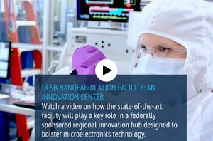
NanoFab Featured in Regional Tech Videos
The UCSB NanoFab is showcased as a driver of innovation and enabler of the regional high-tech industry.
See the videos here:
// John d 09:26, 1 November 2023 (PST)