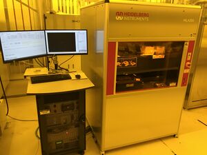
Maskless Aligner (Heidelberg MLA150): Difference between revisions
SOP update |
SOP update |
||
| Line 54: | Line 54: | ||
===Operating Procedures=== |
===Operating Procedures=== |
||
*[https://wiki.nanotech.ucsb.edu/w/images/ |
*[https://wiki.nanotech.ucsb.edu/w/images/c/c0/MLA150_SOP_Rev_K_%28LS%29.pdf MLA150 - Standard Operating Procedure] - updated Jan 5th 2022 |
||
**''Includes File-upload procedure, CAD Conversion, Exposure and Alignment.'' |
**''Includes File-upload procedure, CAD Conversion, Exposure and Alignment.'' |
||
*[[MLA150 - Large Image GDS Generation|Large Image Patterning]] - one way to generate a GDS file out of an arbitrary image (eg. JPG, BMP, PNG etc.) |
*[[MLA150 - Large Image GDS Generation|Large Image Patterning]] - one way to generate a GDS file out of an arbitrary image (eg. JPG, BMP, PNG etc.) |
||
Revision as of 21:10, 2 February 2022
|
About
The MLA150 allows for arbitrary direct-write patterning of I-Line photoresists from an uploaded CAD drawing/file (GDS, DXF, CIF etc.). The system uses a digital micromirror device ("DMD", an array of MEMS mirrors) for patterning the exposure light-field, to programmatically expose digitized patterns directly onto the sample - no glass photomasks/reticles are required.
Depending on the exposure options and write area, the MLA is able to expose a 100mm wafer in about 30min, and achieves minimum features sizes around 0.5µm, with overlay/alignment accuracy better than 200nm.
The system has a continuous, automatic autofocus, using pneumatic and optical detection. This potentially enables lithography on non-planar or curved substrates.
The software allows for custom drawings and aligment marks to be exposed onto any feature located on the microscope.
Greyscale lithography allows for photoresist profiles with repeatable slanted or tapered structures, via an 8-bit greyscale bitmap or layer-structured DXF file.
The high-aspect ratio (variable/long focal length) option enables vertical sidewalls on very thick (~100µm) photoresists.

Detailed Specifications
- Maximum Writeable Area: 150 x 150mm
- Substrate size: 9-inch square or 200mm round down to 5-mm pieces
- Contact staff for pieces < 5 mm.
- Wafer / substrate thickness: Max. 9mm / Min. 0.1mm
- Exposure optics:
- Digital micromirror device (DMD)
- Laser #1: 375nm
- Laser #2: 405nm
- Lens NA = 0.95
- Alignment Accuracy: Global ≤ 500nm; Local ("Field") ≤ 250nm
- Linewidth variation: ≤100nm (relevant to stitched exposure fields)
- Write Grid (Address Unit):
- High Quality Mode (std.): 40nm
- Fast Mode: 100nm
- Additional manufacturer options:
- High-resolution option (Write Mode 1)
- Extended Focus Range
- Variable Focal Depth
- Optical (laser) Autofocus in addition to std. Pneumatic Autofocus
- Greyscale Mode
- (No backside alignment)
Documentation
Operating Procedures
- MLA150 - Standard Operating Procedure - updated Jan 5th 2022
- Includes File-upload procedure, CAD Conversion, Exposure and Alignment.
- Large Image Patterning - one way to generate a GDS file out of an arbitrary image (eg. JPG, BMP, PNG etc.)
Troubleshooting & Known Bugs
- See the above page for troubleshooting/recovery info and workarounds to known bugs.
Video Trainings
Important: You must be authorized by a supervisor to use the tool! The video below is provided for reference only, and does not substitute training by NanoFab staff. Contact the Supervisor for authorization.
- Heidelberg MLA150 Training Video (on GauchoSpace/Panopto)
- UPDATES to the Video Training: please review the addendums below:
- Substrate Templates have been updated, which are currently not reflected in the video.
- Numerous solved issues have been added to the Troubleshooting page.
Design Tools/Info
Recipes
- Recipes > Lithography > Maskless Aligner MLA150
- Starting recipes for various I-Line photoresists
