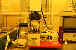
IR Aligner (SUSS MJB-3 IR): Difference between revisions
added additional documentation |
added additional documentation |
||
| Line 45: | Line 45: | ||
*[https://wiki.nanotech.ucsb.edu/wiki/images/d/de/MJB_3_SOP.pdf MJB 3 Standard Operating Procedure] |
*[https://wiki.nanotech.ucsb.edu/wiki/images/d/de/MJB_3_SOP.pdf MJB 3 Standard Operating Procedure] |
||
*[https://wiki.nanotech.ucsb.edu/w/images/1/11/MJB_3_IR_Alignment_Mode_Conversion.pdf MJB 3 Alignment Mode Conversion Procedure] |
*[https://wiki.nanotech.ucsb.edu/w/images/1/11/MJB_3_IR_Alignment_Mode_Conversion.pdf MJB 3 IR Alignment Mode Conversion Procedure] |
||
*[https://wiki.nanotech.ucsb.edu/w/images/1/10/MJB_3_IR_Camera_SOP.pdf MJB 3 IR Camera Operating Procedure] |
|||
Revision as of 16:54, 16 July 2020
|
About
This is a high-performance contact mask aligner with backside alignment capability for opaque materials using IR. It is a versatile, user-friendly compact unit that has a foot print of 600 x 800 mm². The resolution (depending on contact mode, optics and exposure wavelength and "operator technique") is far into the submicron region. The aligner is configured for the near-UV window (365 and 405 nm) and both left and has the "vacuum contact" option extending resolution to ~0.5 microns. Higher resolution optic systems that can be supplied by Suss are given below. The standard soft and hard contact modes of mechanical and pneumatic pressure respectively, only give resolution to 1-2 microns. Exposures can be done on substrates from small "piece parts" of less than 1 cm square to substrates of 3 inch diameter or square. Masks up to 4 inches in size can be used although patterns should be well away from the maskplate edges due to the fact such plates can only be shifted ~ x mm and substrate chuck +/- 3 mm.
Detailed Specifications
- Wafer size: 3" max. for vacuum mode; 4” for soft contact (3” x 3” exposure area)
- Substrate size: 3" x 3" max.
- Wafer / substrate thickness: 0-4.5 mm
- Exposure optics:
- 280-450 nm/200 W mercury lamp (can filter to 350 nm)
- Additional manufacturer options (none installed on our systems):
- DUV (polychromatic): 240-260 nm/350 W Cd-Xe lamp; 0.2 micron resolution (PMMA)
- DUV (monochromatic): 248 nm/KrF excimer laser; 0.3 micron resolution (PMMA)
- 193 nm/ArF excimer laser; 0.2 micron resolution (PMMA)
- Uniformity:
- ±3% over 2" diameter
- ±5% over 3" diameter
Special Notes / Additional Comments
- All units have 200 W mercury lamps
- Infrared Transmission Alignment System
- All models can be equipped for back side alignment using infrared light; this is used when a mask needs to be aligned to features on the substrate backside but exposed to light on the front or resist side
- For processes using this tool please go to the contact lithography process page
- This includes:
- Modified alignment stage
- Motor positioned IR light source under chuck
- Special glass chuck transparent to IR but opaque to UV and visible light
- In-line video camera/monitor for substrate backside viewing and alignment to front-side
- (Note: The vacuum contact mode is not allowed in the ITA System)
