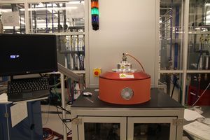
PECVD 2 (Advanced Vacuum): Difference between revisions
(Created page with "{{tool|{{PAGENAME}} |picture=PECVD2.jpg |type = Vacuum Deposition |super= Mike Silva |phone=(805)839-3918x219 |location=Bay 2 |email=silva@ece.ucsb.edu |description = Vision 310 …") |
(No difference)
|
Revision as of 03:41, 1 July 2012
| ||||||||||||||||||||
About
This tool is designed for high quality, precise, reproducible deposition of dielectric films for optical quality films. Metallic material is ion bombarded from a target material and a reactive ion beam of oxygen and/or nitrogen is aimed at the surface, creating a metal-oxide or nitride on the sample.The system is fully computer controlled to facilitate multi-layer stack recipes for high reflectivity or low reflectivity coatings.Current available targets are Ta and Si, with Al and Ti to be added soon.The system is load locked and can handle wafers up to 6” in diameter as well as small pieces. Sample rotation and angling is used to facilitate material quality and allows for sidewall coverage on non-planar surfaces. Uniformity is better than 2% over 4" wafers and reproducibility is expected to be within one percent.
