Help
Uploads by John d
Jump to navigation
Jump to search
This special page shows all uploaded files.
File list
Items per page:
20
50
100
250
500
Username:
Include old versions of files
Show file list
First page
Previous page
Next page
Last page
Date
Name
Thumbnail
Size
Description
Versions
22:10, 16 June 2026
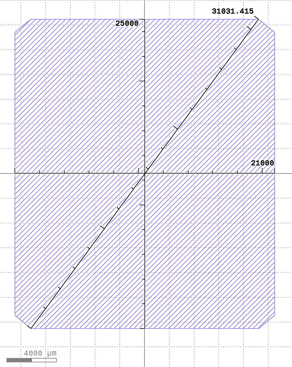
Microscope Training - Epi mode example - 2022-12-21 XYZ W31A after metal --0011.jpg
(
file
)
214 KB
corrected scaling as compared to Dia imaging example
2
20:21, 16 June 2026
Microscope Training - Dia mode example - 2022-12-21 XYZ W31A after metal --0005.jpg
(
file
)
108 KB
1
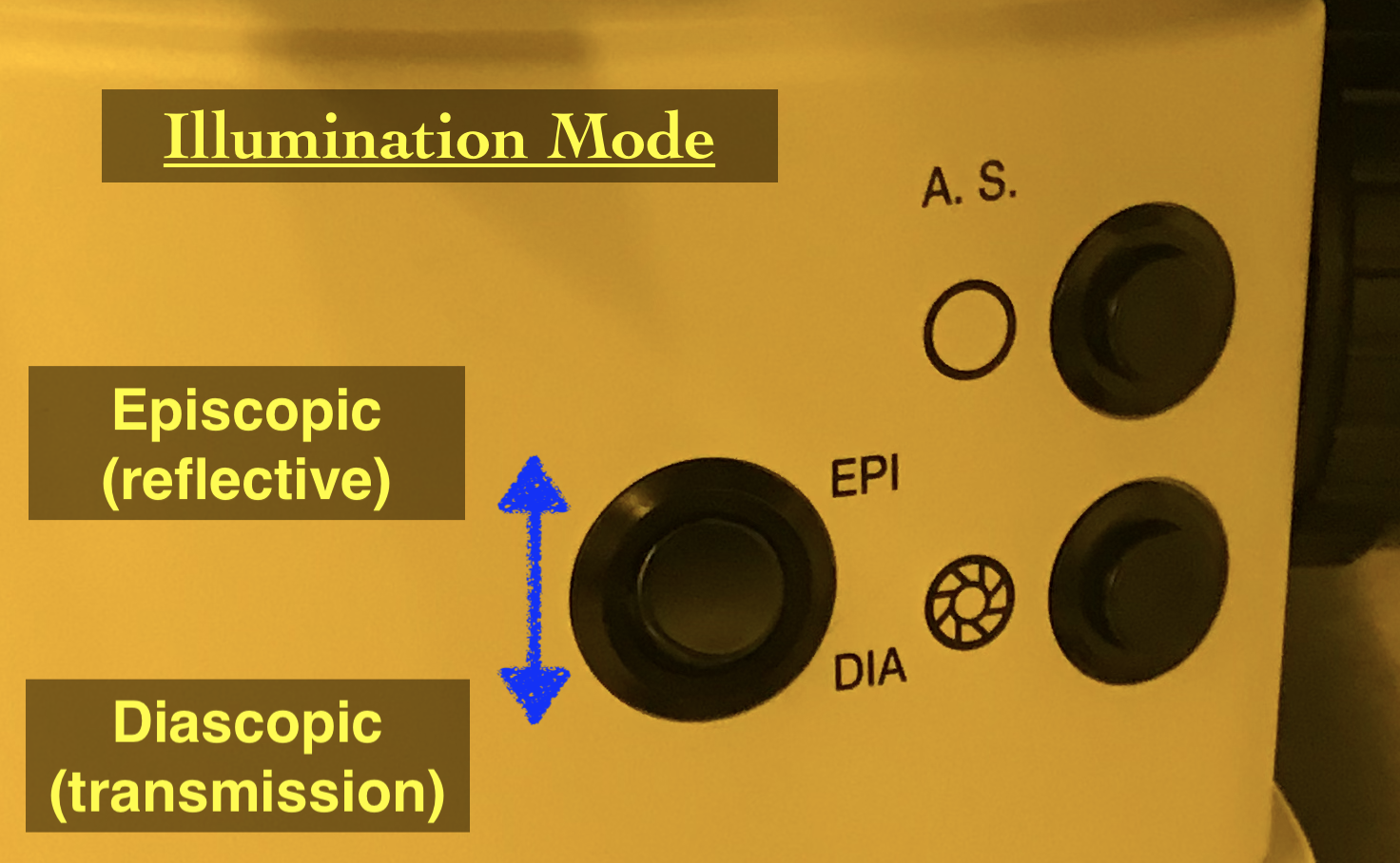
20:13, 16 June 2026
Nikon Microscope Training - front panel Epi Dia switch.png
(
file
)
1.16 MB
1
17:15, 30 April 2026
Vacuum Sealer photo IMG 9946.png
(
file
)
1.41 MB
1
04:56, 19 April 2026
Raith EBPG5150 - Operation Guide.pdf
(
file
)
2.63 MB
SOP for Raith EBPG 5150
1
00:23, 1 April 2026
RaithEBPG 2026-03.png
(
file
)
446 KB
blurred the face
1
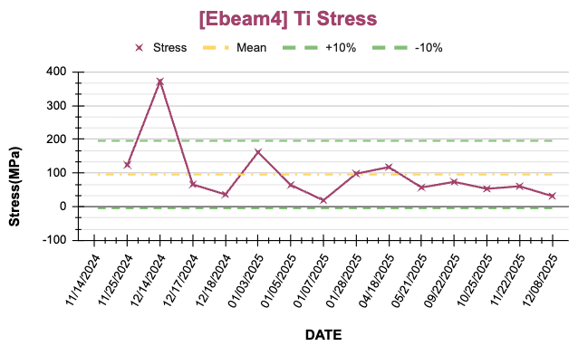
01:33, 12 February 2026
Process Control - E-Beam 4 Titanium Stress plot.png
(
file
)
39 KB
1
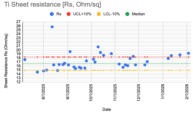
01:29, 12 February 2026
Process Control - Sputter 5 Titanium Sheet Resistance plot.png
(
file
)
43 KB
1
06:17, 26 January 2026
Vernier Template.gds
(
file
)
2 KB
v3: fixed 1st tooth offset, fixed Lyr2 text spacing, added Lyr1/2 cells
5
02:19, 6 December 2025
TOOL actions - example image.jpg
(
file
)
23 KB
screenshot of ToolActions widget
1
23:47, 26 November 2025
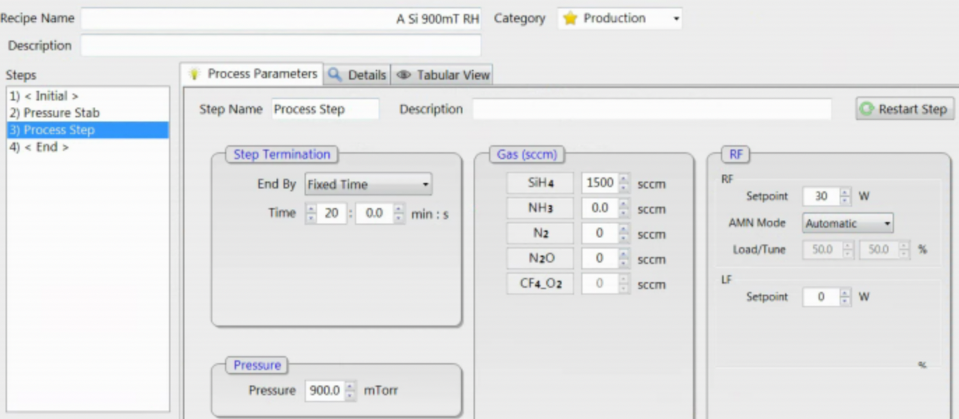
PECVD-2 a-Si Recipe 2025-11.png
(
file
)
639 KB
1
02:56, 20 November 2025
IR Alignment check 01 - crop.png
(
file
)
5.69 MB
Reverted to version as of 19:04, 1 March 2024 (UTC)
3
23:21, 19 November 2025
MJB-IR - squares alignment and field of view.png
(
file
)
65 KB
1
00:16, 12 August 2025
ASML Dose vs Hole Diam - AT230829.png
(
file
)
76 KB
1
06:47, 5 August 2025
Tutorial - Photomasks - GCA example template (incorrect, guessed coords) v1.png
(
file
)
204 KB
2
06:46, 5 August 2025
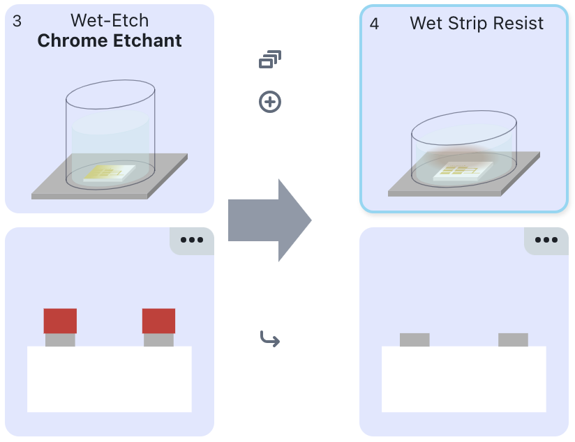
Tutorial - photomasks - Cr etch and PR strip.png
(
file
)
59 KB
2
06:45, 5 August 2025
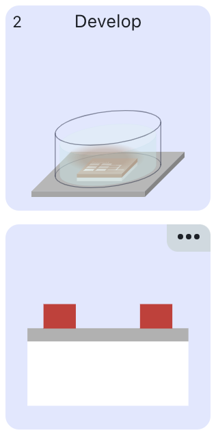
Tutorial - Photomasks - Develop.png
(
file
)
28 KB
2
06:44, 5 August 2025
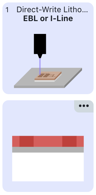
Tutorial - Photomasks - direct-write.png
(
file
)
21 KB
2
06:43, 5 August 2025
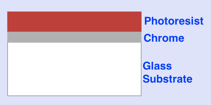
Tutorial - Photomask - Substrate.png
(
file
)
27 KB
better labelling
2
05:36, 29 July 2025
Contact-AlignMarks Vernier DemisDJohn v5 screenshot overlay.png
(
file
)
66 KB
transparent Lyr1
2
05:16, 29 July 2025
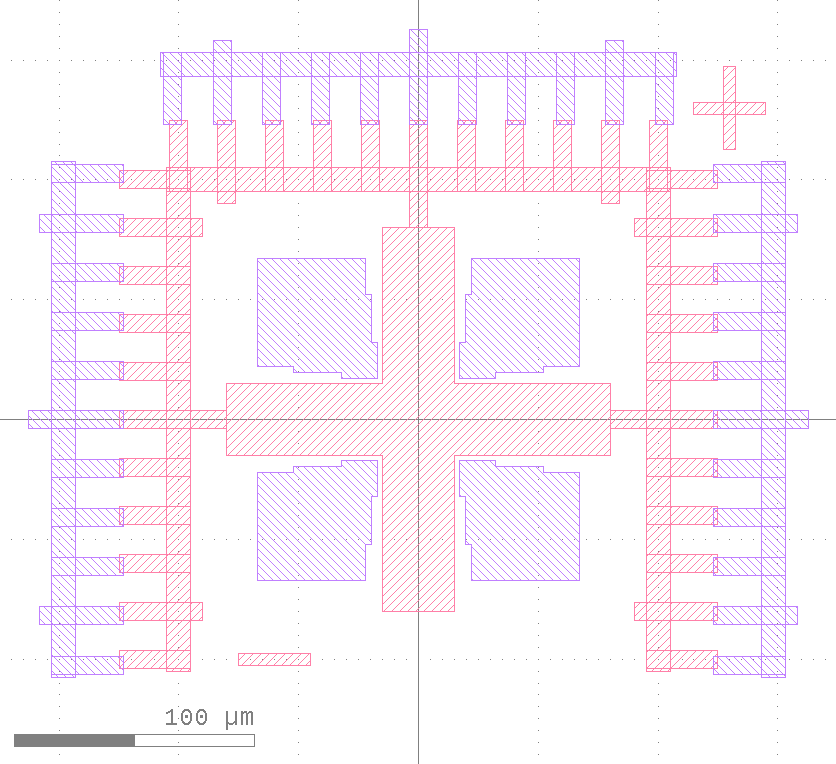
Contact-AlignMarks Vernier DemisDJohn v5.gds
(
file
)
5 KB
Contact Alignment Marks redesigned by Demis D. John - OASIS
1
05:14, 29 July 2025
Contact-AlignMarks Vernier DemisDJohn v5.oas
(
file
)
1 KB
1
05:11, 29 July 2025
Contact-AlignMarks Vernier DemisDJohn v3 Screenshot.png.png
(
file
)
606 KB
now shows all 3 Cells with names
3
16:41, 18 June 2025
KLayout - auto-load layer properties screenshot.png
(
file
)
23 KB
1
01:48, 29 April 2025
ASML Reticle Programming Params - DEMIS-DOE v1.xlsx
(
file
)
11 KB
Stepper reticle tutorial - programming sheet for DOE layouts (Demis D John)
1
01:47, 29 April 2025
CAD Tutorial for ASML Reticle v2 DEMIS-DOE.OAS
(
file
)
2 KB
Stepper reticle tutorial OAS file (Demis D John)
1
01:26, 29 April 2025
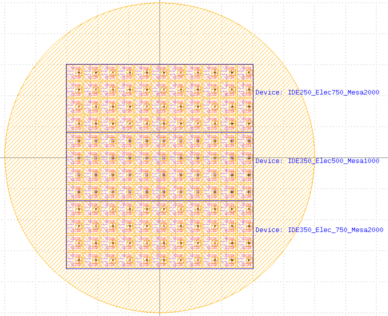
Stepper Reticle Layout Tutorial - Wafer layout with variations.png
(
file
)
95 KB
1
01:24, 29 April 2025
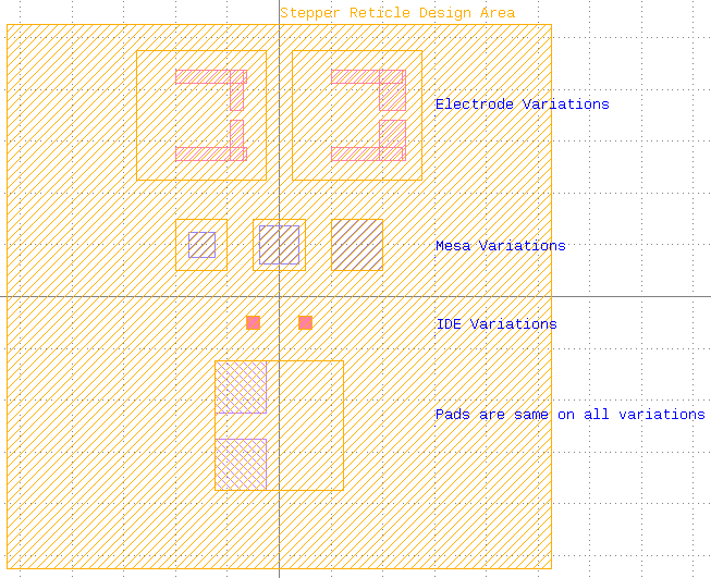
Stepper Reticle Layout Tutorial - Reticle layout with variations.png
(
file
)
42 KB
1
20:15, 12 April 2025
Edge bead Removal on MA6 - IMG 5625 - placed on wafer.jpg
(
file
)
1.63 MB
1
20:14, 12 April 2025
Edge bead Removal on MA6 - IMG 5626 - place on wafer.jpg
(
file
)
1.89 MB
1
20:13, 12 April 2025
Edge bead Removal on MA6 - IMG 5624 - cassette location.jpg
(
file
)
3.65 MB
1
20:12, 12 April 2025
Edge bead Removal on MA6 - IMG 5623 - vidmar drawers.jpg
(
file
)
2.75 MB
1
20:27, 7 April 2025
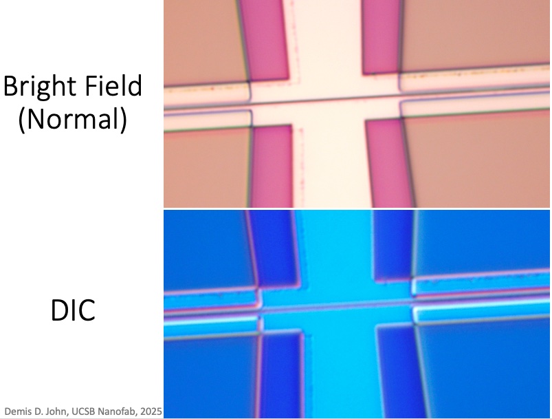
Microscope DIC-Nomarski Example v1.jpg
(
file
)
84 KB
1
20:15, 7 April 2025
Dark Field Microscopy - High Particle Count example 2025-03-25 W1 particle check Demis.jpg
(
file
)
789 KB
1
20:10, 7 April 2025
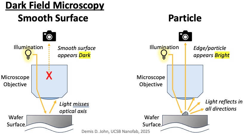
Dark Field Microscopy explanation v1.jpg
(
file
)
82 KB
1
19:13, 11 March 2025
Nanofabrication Facility Project Description.xlsx
(
file
)
33 KB
added UC Billing Recharge line
6
18:40, 9 March 2025
FL-ICP 50W SiO2 etch with Ru Hard Mask.png
(
file
)
936 KB
1
18:39, 9 March 2025
FL-ICP 200W SiO2 Etch with Ru Hardmask - Ning Cao.png
(
file
)
1.15 MB
cross section instead of 30° view
2
02:02, 2 March 2025
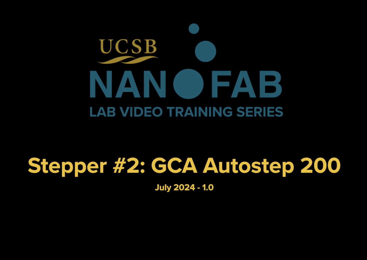
GCA Autostep 200 training vid title screen.png
(
file
)
239 KB
added play button overlay
2
22:11, 21 February 2025
ASML Mask Design Area.png
(
file
)
96 KB
1
23:36, 7 February 2025
ASML OPC - Skyler Palatnik 060224 PR vtxHvP 23mJ NO OPC 1.png
(
file
)
839 KB
1
23:34, 7 February 2025
ASML OPC - Skyler Palatnik 060224 PR vtxHvP 15mJOPC 3.png
(
file
)
773 KB
1
00:50, 7 February 2025
PECVD1 SiO2 F50 WaferMap example.jpg
(
file
)
1.04 MB
1
00:46, 7 February 2025
PECVD SPC Chart Example.png
(
file
)
269 KB
1
23:39, 6 February 2025
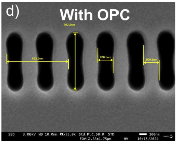
ASML SEM DBR With OPC .png
(
file
)
92 KB
1
23:38, 6 February 2025
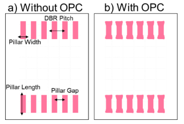
ASML SEM DBR without OPC.png
(
file
)
113 KB
1
23:37, 6 February 2025
ASML OPC CAD.png
(
file
)
34 KB
1
23:30, 3 January 2025
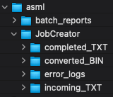
ASML JobCreator FTP Folders 01.png
(
file
)
10 KB
1
22:51, 18 December 2024
EB-1 4-wf fixture 04 fixture loaded in chamber.jpg
(
file
)
1.23 MB
1
22:48, 18 December 2024
EB-1 4-wf fixture 03 wafers inserted.jpg
(
file
)
1.08 MB
1
First page
Previous page
Next page
Last page
Navigation menu
Personal tools
Create account
Log in
Namespaces
Special page
English
Views
More
Search
InvisibleMenu
QuickLinks
Lab Rules
Common Questions/FAQ
Staff List
Equipment Signup
Chemicals + MSDS
Equipment
Full Tool List
Lithography
Vacuum Deposition
Dry Etch
Wet Processing
Thermal Processing
Packaging
Metrology & Test
Recipes and Data
Lithography
Vacuum Deposition
Dry Etching
Wet Etching
Thermal Processing
Packaging Tools
Data + Info
Process Control Data
Tutorials
Calculators/Utilities
NanoFab Info
Research + Pubs
Tech Talks
Tools
User contributions
Logs
View user groups
Special pages
Printable version


_v1.png)


