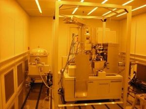
E-Beam Lithography System (JEOL JBX-6300FS): Difference between revisions
Jump to navigation
Jump to search
Mitchell b (talk | contribs) |
Mitchell b (talk | contribs) |
||
| Line 39: | Line 39: | ||
*Dynamic Focus and Stigmation Control for improved writing performance across the entire scan field. |
*Dynamic Focus and Stigmation Control for improved writing performance across the entire scan field. |
||
*UNIX computer controlled |
*UNIX computer controlled |
||
*Advanced Fracturing software available (Layout BEAMER from GeniSys, Inc) |
*Advanced Fracturing software available (Layout BEAMER from GeniSys, Inc) |
||
Revision as of 17:43, 31 October 2017
|
About
The 6300FS machine was installed at UCSB in May 2007.
This system uses the vector scan approach for electron beam deflection within a field, step and repeat for stage movement between fields, the combination of which allows the entire area of the sample to be exposed to the electron beam.
The machine can be run at 25, 50 and 100 kV. Note however that only the 100kV mode is used at UCSB.
Applications
- Quantum devices in AlGaAs/GaAs heterostructures
- Photonic crystal production for various photonic band-gap applications
- sub-50nm gates for T-Gate production in AlGaN/GaN HEMT structures
- micro-ring resonator structures for photonic waveguide filtering
- DBR gratings for 1.5 um lasers
- Aligned nano-electrode fabrication for various nanowire/nanotube electronic measurements
- Nano-MEMS structures
- 100 nm T-Gates for millimeter wave hererojunction FETs
Detailed Specifications
- Utilizes a “Hi-brightness” thermal field emission electron source (ZnO/W) with a minimum spot-size at the substrate of 2nm; operates at 100kV only
- Unique two lens/deflector scanning system:
- 4th lens => 20-25nm minimum line-width, 1.000nm scan step resolution, 500 x 500um scan field
- 5th lens => 7-8 nm minimum line-width, 0.125nm scan step resolution, 62.5x62.5um scan field
- Maximum deflector scan speed = 25MHz (=> 40ns/pixel minimum dwell time)
- 150x150 mm writable area; stage position control to 0.6nm accuracy (λ/1024); 10mm/s maximum stage speed
- Dynamic Focus and Stigmation Control for improved writing performance across the entire scan field.
- UNIX computer controlled
- Advanced Fracturing software available (Layout BEAMER from GeniSys, Inc)
- automated proximity correction of patterns possible
- ability to manually position write fields within a pattern for optimum inter-field writing performance
- ability to adjust beam scanning strategy within a write field for optimum intra-field writing performance
- fine tuning of line-edge roughness by shot pitch correction
Electron Beam Resists
Currently available at UCSB are:
- PMMA: (950K in anisole, 950K in MIBK, 495K in anisole, 50K in anisole): very high-resolution positive polymer-based resist with relatively poor sensitivity (resolution scales directly and sensitivity scales inversely with molecular weight); very poor plasma etch resistance, hence used primarily to fabricate metal lines via liftoff processes (via a bi-layer resist scheme...low MW on bottom, high MW on top for single lines, or vice-versa for T-gate fabrication); utilizes an inert solvent developer (usually MIBK:IPA mixtures)
- P(MMA-MAA) copolymer: (low MW methyl-methacrylate (MMA) and methacrylic acid (MAA) copolymers in ethyl lactate): a positive polymer-based resist with poor resolution but with significantly higher sensitivity than the higher MW PMMA resists above; used primarily as the top layer in a bi-layer resist scheme for T-Gate fabrication, and utilizes inert solvent developer (MIBK:IPA mixtures)
- CSAR-62: ZEP-equivalent resist manufactured in Germany at much more competitive pricing!; very high-resolution polymer-based positive resist with very good sensitivity and excellent etch resistance; can be used in both metal lift-off processes (slight overexposure results in an excellent undercut profile) and various dry-etch processes for pattern transfer to the underlying substrate; utilizes inert solvent developers (e.g., n-amyl acetate for higher sensitivity and good resolution or MIBK:IPA mixtures for increased LER performance)
- maN-2403: negative polymer-based resist (that is NOT chemically amplified) with very good resolution (down to the 40-50nm range) and sensitivity; exhibits excellent dry-etch resistance; developed using a dilute basic solution (e.g., metal-ion-free developers such as AZ-300MIF)
- HSQ: negative resist that is based on spin-on glass material (ie, not polymer-based) with extremely good resolution (features below 10nm can be resolved); etch resistance is high in Cl-based chemistries since HSQ reduces to a porous SiOx structure after exposure and development; sensitivity and contrast are very dependent on developer solution used and are usually poor - standard AZ300MIF developer solutions have decent sensitivity (100's of uC/cm2 at 100kV) but extremely poor contrast, stronger (and toxic!) 25%TMAH solutions have much better contrast but poor sensitivity (1000's of uC/cm2 at 100kV), "salty" developer solutions using 1wt% NaCl dissolved in either 4wt% NaOH or AZ300MIF solutions have the best contrast but reduce sensitivity significantly (10,000's of uC/cm2 at 100kV)
- UV6/UVN-210: chemically amplified polymer-based resists with high resolution and excellent sensitivity (clearing doses below 100uC/cm2 at 100kV); UV6 used mostly in optimized t-gate resist structures; developed using a dilute basic solution (e.g., metal-ion-free developers such as AZ-300MIF)
