Fluorine ICP Etcher (PlasmaTherm/SLR Fluorine ICP): Difference between revisions
m John d moved page Si Deep RIE (PlasmaTherm/Bosch Etch) to Fluorine ICP Etcher (PlasmaTherm/SLR Fluorine ICP): tool converted |
note indicate info is from pre-conversion |
||
| Line 1: | Line 1: | ||
Note: This page needs to updated - it is still showing old information from before it was converted to a Fluorine etcher. It is not a Silicon Bosch Etcher any more. |
|||
{{tool|{{PAGENAME}} |
{{tool|{{PAGENAME}} |
||
|picture=SiDeep.jpg |
|picture=SiDeep.jpg |
||
| Line 11: | Line 12: | ||
|toolid=28 |
|toolid=28 |
||
}} |
}} |
||
= About = |
= About = |
||
| Line 35: | Line 37: | ||
= Recipes = |
= Recipes = |
||
Etch recipes can be found on the following page: [[ICP_Etching_Recipes#Si_Deep_RIE_.28PlasmaTherm.2FBosch_Etch.29 | Dry Etching Recipes > Si Deep RIE (PlasmaTherm/Bosch Etch) |
Etch recipes can be found on the following page: [[ICP_Etching_Recipes#Si_Deep_RIE_.28PlasmaTherm.2FBosch_Etch.29 | Dry Etching Recipes > Si Deep RIE (PlasmaTherm/Bosch Etch)]] |
||
Revision as of 21:53, 28 August 2018
Note: This page needs to updated - it is still showing old information from before it was converted to a Fluorine etcher. It is not a Silicon Bosch Etcher any more.
| |||||||||||||||||||||
About
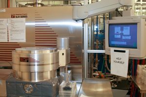
The Si DRIE system is a Plasma-Therm 770 SLR series system with a loadlock. The system has an Inductively Coupled Plasma (ICP) coil and a capactively coupled substrate RF supply to independently control plasma density and ion energy in the system. This system is dedicated to deep etching in silicon for MEMs structures. The Bosch process is used for obtaining deep, vertical, high aspect ratio structures. This process cycles between a polymer deposition cycle using C4F8 gas and no substrate bias, and an etching cycle using a SF6 / Ar mixture with substrate bias. The system is fully computer controlled in all aspects of the pumping cycles and process control, and can be programmed by the user. The fixturing is configured for 4" diameter Si wafers and uses a clamp to hold the sample on the RF chuck.
The materials allowed in the system are limited to Silicon, SiO2, Si3N4, SiOXNY, and polymer films such as photoresist, PMMA, and polyimide. Other materials can be placed in the chamber, such as metal layers on the surface, only if they will remain completely protected from the plasma by an allowed material during the entire etch. Some alternate stop-etch materials may be allowed upon discussion with facility staff.
Helium back-side cooling is used to keep the sample cool during the etch. Temperature control is very important as the polymer passivation layer is chemically etched away by the fluorine gas at elevated temperatures, resulting in loss of profile control. Pieces of wafers can be mounted onto 4" silicon wafers using thin, uniform, bubble-free hard baked photoresist. The etch rate is dependent on the open area of silicon (macro-loading effect) with large open area samples etching slower than small open area samples. Features with a high aspect ratio will also etch slower than more open areas. This is known as RIE lag or the micro-loading effect.
Detailed Specifications
- 1000 W ICP coil power at 2 MHz and 500 W substrate bias at 13.56 MHz plasma generators
- C4F8, SF6, O2, Ar, N2 gases available
- He-back-side cooling
- Windows-based computer control of process and wafer handling
- Allowed materials: Silicon, SiO2, Si3N4, SiOXNY, and polymer films such as photoresist, PMMA, and polyimide; other stop-etch materials on request
- Realized etch rates (including passivation steps) of > 3 um / min. Using the standard Plasma Therm recipe, a nominal etch rate of 2 um / min. is achieved; etch rate dependent on conditions and open area
- Laser monitoring with camera and etch simulation software for SOI etching - Intellemetrics
Documentation
Recipes
Etch recipes can be found on the following page: Dry Etching Recipes > Si Deep RIE (PlasmaTherm/Bosch Etch)
