Automated Coat/Develop System (S-Cubed Flexi): Difference between revisions
Jump to navigation
Jump to search
(added link to SOP) |
(Text replacement - "/wiki/index.php/" to "/wiki/index.php?title=") |
||
| Line 39: | Line 39: | ||
*Recipe Page for S-Cubed Coater: [[Lithography Recipes#Automated%20Coat.2FDevelop%20System%20Recipes%20.28S-Cubed%20Flexi.29|Lithography Recipes > Automated Coat/Develop System Recipes (S-Cubed Flexi]]) |
*Recipe Page for S-Cubed Coater: [[Lithography Recipes#Automated%20Coat.2FDevelop%20System%20Recipes%20.28S-Cubed%20Flexi.29|Lithography Recipes > Automated Coat/Develop System Recipes (S-Cubed Flexi]]) |
||
*See the [https://wiki.nanotech.ucsb.edu/wiki/index.php |
*See the [https://wiki.nanotech.ucsb.edu/wiki/index.php?title=Lithography_Recipes#Chemicals_Stocked_.2B_Datasheets Photolith. Chemicals page] for info on the installed resists. |
||
=Operating Procedures= |
=Operating Procedures= |
||
Revision as of 19:46, 4 September 2021
| |||||||||||||||||||||||
THIS TOOL IS ONLY FOR STAFF USE AT THIS TIME.
About
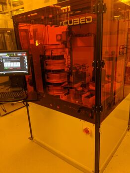
The S3-Coater is a Coater/Developer system that has one photoresist spinner, one developer spinner and 4 hotplates each with independent temperature control and a chill plate. A central robot picks your wafer/s from one of 2 cassettes, processes them and returns them to the cassette. The system is recipe driven with a high degree of process control and minimal backside contamination, and coats photoresists with low particle counts/streaks and high uniformity.
At this time only full size substrates are allowed on this system. The S3 Coater is still in process development and not open for general use.
Detailed Specifications
- Wafer Size: 100mm (150mm possible but not set up)
- PR Coating Properties:
- Uniformity < 1.0%
- < 100 particles on 100mm wafer
- Photoresists/Underlayers Available:
- UV6-0.8
- DS-K101-304
- PMMA
- PMGI SF11
- PMGI SF5
- Solvents Available:
- EBR100
- Developers Available:
- AZ 300 MiF
Process Information
- Recipe Page for S-Cubed Coater: Lithography Recipes > Automated Coat/Develop System Recipes (S-Cubed Flexi)
- See the Photolith. Chemicals page for info on the installed resists.
Operating Procedures
- Standard Operating Procedure - For running pre-written recipes only.
