Plasma Activation (EVG 810): Difference between revisions
Jump to navigation
Jump to search
(Text replacement - "www.nanotech.ucsb.edu/wiki/" to "wiki.nanotech.ucsb.edu/wiki/") |
(SOP update) |
||
| Line 18: | Line 18: | ||
*Gases used: O<sub>2</sub> and N<sub>2</sub> |
*Gases used: O<sub>2</sub> and N<sub>2</sub> |
||
*Sample size: pieces to 6” wafer |
*Sample size: pieces to 6” wafer |
||
*Max power: 200W |
|||
*Recipes characterized for substrate thicknesses between 250um and 750um. Thicknesses outside of this range need to have parameters optimized to minimize reflective power. |
*Recipes characterized for substrate thicknesses between 250um and 750um. Thicknesses outside of this range need to have parameters optimized to minimize reflective power. |
||
==Documentation== |
==Documentation== |
||
*[https://wiki.nanotech.ucsb.edu/ |
*[https://wiki.nanotech.ucsb.edu/w/images/3/37/EVG_Plasma_Activation_SOP_Rev_C.pdf Plasma Activation Standard Operating Procedure] |
||
*[https://wiki.nanotech.ucsb.edu/wiki/images/9/93/EVG_Plasma_Activation_Recipe_Copying.pdf How to copy recipes] |
*[https://wiki.nanotech.ucsb.edu/wiki/images/9/93/EVG_Plasma_Activation_Recipe_Copying.pdf How to copy recipes] |
||
Revision as of 17:25, 3 January 2022
| |||||||||||||||||||||
About
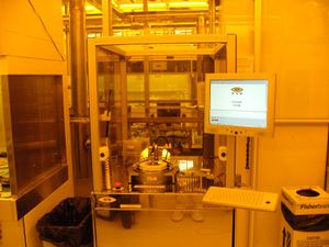
This a capacitively coupled Oxygen plasma activation system used exclusively for the surface activation of clean surfaces prior to wafer bonding. This technique allows bonding temperatures to be lowered and is used as a companion tool to the Karl-Suss SB6 wafer bond tool.
Detailed Specifications
- Gases used: O2 and N2
- Sample size: pieces to 6” wafer
- Recipes characterized for substrate thicknesses between 250um and 750um. Thicknesses outside of this range need to have parameters optimized to minimize reflective power.
Documentation
Recipes
Please see the Oxygen Plasma Recipe page for standard EVG recipes.
