Chemical-Mechanical Polisher (Logitech): Difference between revisions
Jump to navigation
Jump to search
Content deleted Content added
Created page with "{{tool|{{PAGENAME}} |picture=XeF2.jpg |type = Dry Etch |super= Wet Processing |phone=(805)839-3918x216 |location=Bay 5 |email=freeborn@ece.ucsb.edu |description = ORBIS Chemical …" |
No edit summary |
||
| (10 intermediate revisions by 5 users not shown) | |||
| Line 1: | Line 1: | ||
{{ |
{{tool2|{{PAGENAME}} |
||
|picture= |
|picture=CMP.jpg |
||
|type = Dry Etch |
|type = Dry Etch |
||
|super= |
|super= Bill Millerski |
||
|super2= Don Freeborn |
|||
|phone=(805)839-3918x216 |
|phone=(805)839-3918x216 |
||
|location=Bay 5 |
|location=Bay 5 |
||
| Line 9: | Line 10: | ||
|manufacturer = [http://www.logitech.uk.com/products-solutions/products-and-accessories.aspx Logitech] |
|manufacturer = [http://www.logitech.uk.com/products-solutions/products-and-accessories.aspx Logitech] |
||
|materials = |
|materials = |
||
|toolid=50 |
|||
}} |
}} |
||
= |
=About= |
||
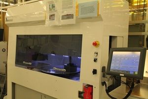
The Logitech Orbis system is used in the facility for fine-scale polishing and planarization of a variety of materials including glass, silicon, GaAs, InP, GaN, etc. Wafers up to 6” diameter can be polished on the system. |
The Logitech Orbis system is used in the facility for fine-scale polishing and planarization of a variety of materials including glass, silicon, GaAs, InP, GaN, etc. Wafers up to 6” diameter can be polished on the system. |
||
Several slurries and pads are available to provide a range of polishing options depending on the material being processed. Pieces can also be handled on the system by wax-mounting with the [[Wafer Bonder (Logitech WBS7)|Logitech Bonder]]. |
|||
Each process is often unique in geometry and material combinations so that independent process development is required for most CMP applications. |
|||
=[[Instructions]]= |
|||
https://wiki.nanotech.ucsb.edu/w/images/c/c0/CMP.pdf |
|||
Latest revision as of 18:03, 30 August 2022
| ||||||||||||||||||||||||||||||
About
The Logitech Orbis system is used in the facility for fine-scale polishing and planarization of a variety of materials including glass, silicon, GaAs, InP, GaN, etc. Wafers up to 6” diameter can be polished on the system.
Several slurries and pads are available to provide a range of polishing options depending on the material being processed. Pieces can also be handled on the system by wax-mounting with the Logitech Bonder.
Each process is often unique in geometry and material combinations so that independent process development is required for most CMP applications.
