IBD: Calibrating Optical Thickness: Difference between revisions
Jump to navigation
Jump to search
(minor corrections) |
(added publication policy) |
||
| Line 6: | Line 6: | ||
##For example, if SiO2 measured at 5.2nm/min and RIX is n<sub>1550</sub> = 1.494, then ''SiO 1/4λ thickness: d<sub>1/4λ</sub> = 1550nm / 4 / 1.494 = 259.4nm'' '''''SiO 1/4λ time''': t<sub>1/4λ</sub> = 259.4nm ÷ 5.2nm/min = 49.88min = '''2993.077 sec''''' (and do the same for TaO) |
##For example, if SiO2 measured at 5.2nm/min and RIX is n<sub>1550</sub> = 1.494, then ''SiO 1/4λ thickness: d<sub>1/4λ</sub> = 1550nm / 4 / 1.494 = 259.4nm'' '''''SiO 1/4λ time''': t<sub>1/4λ</sub> = 259.4nm ÷ 5.2nm/min = 49.88min = '''2993.077 sec''''' (and do the same for TaO) |
||
#Deposit a fabry-perot 1/2-λ of one film (SiO or TaO) cavity onto a Silicon piece, using the above 1/4-λ times (aka. SiO/4 or TaO/4), to calibrate that film's optical-thickness. |
#Deposit a fabry-perot 1/2-λ of one film (SiO or TaO) cavity onto a Silicon piece, using the above 1/4-λ times (aka. SiO/4 or TaO/4), to calibrate that film's optical-thickness. |
||
##eg. for SiO Fabry-Perot cavity (aka. SiO-FP) ''SiO/4 + TaO/4 + SiO/4 + TaO/4 + SiO/4 + TaO/4 + ('''SiO/4 + SiO/4''') + TaO/4 + SiO/4 + TaO/4 + SiO/4 + TaO/4'' |
##eg. for SiO Fabry-Perot cavity (aka. SiO-FP) ''SiO/4 + TaO/4 + SiO/4 + TaO/4 + SiO/4 + TaO/4 + ('''SiO/4 + SiO/4''') + TaO/4 + SiO/4 + TaO/4 + SiO/4 + TaO/4'' |
||
##Here we used only 3 periods of DBR on either side of the 1/2-λ cavity, to speed up the deposition. |
##Here we used only 3 periods of DBR on either side of the 1/2-λ cavity, to speed up the deposition. |
||
#Measure the reflectivity on [[Optical Film Spectra + Optical Properties (Filmetrics F10-RT-UVX)|Filmetrics F10-RT]]. |
#Measure the reflectivity on [[Optical Film Spectra + Optical Properties (Filmetrics F10-RT-UVX)|Filmetrics F10-RT]]. |
||
| Line 13: | Line 13: | ||
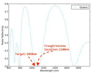
###Here is an example of a Fabry-Perot cavity that was targeting a 1050nm, and measured a 1100nm trough:[[File:IBD SiO-FP - long 1100nm - Reflectivity Spectrum (EMpy).png|alt=Simulated plot of SiO-FP reflectivity, for a 1050nm target but measured trough at 1100nm|none|thumb|Example: Targeting a 1050nm SiO-FP, the measured trough location is at 1100nm. ]](In this case, one would apply a correction to the SiO/4 time by multiplying by ''1050÷1000''.) |
###Here is an example of a Fabry-Perot cavity that was targeting a 1050nm, and measured a 1100nm trough:[[File:IBD SiO-FP - long 1100nm - Reflectivity Spectrum (EMpy).png|alt=Simulated plot of SiO-FP reflectivity, for a 1050nm target but measured trough at 1100nm|none|thumb|Example: Targeting a 1050nm SiO-FP, the measured trough location is at 1100nm. ]](In this case, one would apply a correction to the SiO/4 time by multiplying by ''1050÷1000''.) |
||
#Correct the film's optical thickness as so: |
#Correct the film's optical thickness as so: |
||
##t<sub>1/4λ</sub> * λ<sub>target</sub> / λ<sub>measured</sub> = ''corrected'' t<sub>1/4λ</sub> |
##t<sub>1/4λ</sub> * λ<sub>target</sub> / λ<sub>measured</sub> = ''corrected'' t<sub>1/4λ</sub> |
||
##2993.077 sec * (1550nm / 1600nm) = '''2899.543 sec''' for SiO/4 layers |
##2993.077 sec * (1550nm / 1600nm) = '''2899.543 sec''' for SiO/4 layers |
||
###Use this corrected time for all SiO/4 layers. |
###Use this corrected time for all SiO/4 layers. |
||
| Line 27: | Line 27: | ||
<br /> |
<br /> |
||
Developed by Demis D. John, Bob Farrell, Dustin Kleckner, ~2008-2010. This is the same method used by UCSB VCSEL groups years earlier, for calibrating VCSEL MOCVD/MBE growths. |
Developed by Demis D. John, Bob Farrell, Dustin Kleckner, ~2008-2010. This is the same method used by UCSB VCSEL groups years earlier, for calibrating VCSEL MOCVD/MBE growths. Please consider our [[Frequently Asked Questions#Publications acknowledging the Nanofab|<u>publication policy</u>]] if you publish papers using this information. |
||
Revision as of 00:03, 16 September 2023
Basic method for calibrating optical thickness, for DBR/multi-layer optical coatings (2 films only). Commonly used for SiO2/TaO DBR mirrors.
- Get dep rate & refractive index (RIX) of individual SiO and TaO films, using single-deps and J.A. Woolam Ellipsometer or equivalent tool. Approx. rate from previous user is also acceptable.
- Get RIX at the target wavelength, using "Derived Params" on JAW or Cauchy equation A/B/C params. For example, if targeting a DBR centered at 1550nm (target λ=1550nm), you will want to know the RIX at 1550nm specifically.
- Calculate approximate dep. time to achieve a 1/4-wave thickness at the target wavelength, for each film (SiO and TaO).
- For example, if SiO2 measured at 5.2nm/min and RIX is n1550 = 1.494, then SiO 1/4λ thickness: d1/4λ = 1550nm / 4 / 1.494 = 259.4nm SiO 1/4λ time: t1/4λ = 259.4nm ÷ 5.2nm/min = 49.88min = 2993.077 sec (and do the same for TaO)
- Deposit a fabry-perot 1/2-λ of one film (SiO or TaO) cavity onto a Silicon piece, using the above 1/4-λ times (aka. SiO/4 or TaO/4), to calibrate that film's optical-thickness.
- eg. for SiO Fabry-Perot cavity (aka. SiO-FP) SiO/4 + TaO/4 + SiO/4 + TaO/4 + SiO/4 + TaO/4 + (SiO/4 + SiO/4) + TaO/4 + SiO/4 + TaO/4 + SiO/4 + TaO/4
- Here we used only 3 periods of DBR on either side of the 1/2-λ cavity, to speed up the deposition.
- Measure the reflectivity on Filmetrics F10-RT.
- Locate the wavelength of the minimum (dip) in the optical spectrum. Spectrum will typically be very broad, due to omitting many of the DBR layers for speed.
- For example, the trough might show a minimum at 1600nm instead of the targeted 1550nm.
- Here is an example of a Fabry-Perot cavity that was targeting a 1050nm, and measured a 1100nm trough:(In this case, one would apply a correction to the SiO/4 time by multiplying by 1050÷1000.)
- For example, the trough might show a minimum at 1600nm instead of the targeted 1550nm.
- Correct the film's optical thickness as so:
- t1/4λ * λtarget / λmeasured = corrected t1/4λ
- 2993.077 sec * (1550nm / 1600nm) = 2899.543 sec for SiO/4 layers
- Use this corrected time for all SiO/4 layers.
- Do the same Fabry-Perot correction for the other film, in this case TaO-FP, and apply the new TaO/4 time to the recipe.
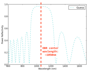
- Perform a test-DBR deposition onto Silicon, eg. 9 periods (less than full, which could be 15 periods or more), and measure on Filmetrics F10-RT, to confirm that center wavelength is in the right spot. An example DBR test-dep targeting 1050nm looks like this:
- Perform full-DBR deposition onto production parts. Include a flat Silicon witness for measuring the final DBR reflectivity spectrum.
- Sources of error: thick, stressy films exhibit the stress-optic effect, in which compressed films (closer to the substrate) will often show a reduction in RIX. In going from a 9-period DBR to a 18-period DBR, you might see a ~10-20nm blue-shift. Some users for who such a shift is outside the device tolerance will do a full DBR dep, then apply a % reduction to all dep times to further dial in the DBR reflectivity band.
- The same method can be used to calibrate optical-thickness for arbitrary multi-layer optical filters.
Note, you can verify/better understand the above method using any electromagnetic thin-film simulator. For example, EMpy has a simple transfer-matrix example for doing this, along with RIX models contributed by Demis. Demis created the above simulations using EMpy.
Developed by Demis D. John, Bob Farrell, Dustin Kleckner, ~2008-2010. This is the same method used by UCSB VCSEL groups years earlier, for calibrating VCSEL MOCVD/MBE growths. Please consider our publication policy if you publish papers using this information.

