Laser Etch Monitoring: Difference between revisions
added examples of etch monitoring |
|||
| (9 intermediate revisions by the same user not shown) | |||
| Line 3: | Line 3: | ||
|type = Dry Etch |
|type = Dry Etch |
||
|super= Demis D. John |
|super= Demis D. John |
||
|location=ICP1, ICP2, Fluorine Etcher, DSE-iii |
|location=ICP1, ICP2, Fluorine Etcher, DSE-iii, Oxford Cobra |
||
|description = Laser Endpoint Detection for Dry Etching |
|description = Laser Endpoint Detection for Dry Etching |
||
|manufacturer = Intellemetrics |
|manufacturer = Intellemetrics |
||
| Line 9: | Line 9: | ||
}} |
}} |
||
==Overview== |
==Overview== |
||
A number of our dry etching systems have Laser Etch monitors installed, for "endpoint detection". These systems allow you to end your etch at a known etch depth, or within a certain layer (with some caveats). This nearly eliminates the need to calibrate etch rates or to use timed etching only, which is especially important in our lab where etch rates can vary depending on the previous etches performed in the chamber. |
A number of our dry etching systems have Laser Etch monitors installed, for "endpoint detection". These systems allow you to end your etch at a known etch depth, or within a certain layer (with some caveats). They provide optical feedback "live" during the etch, allowing you to make the decision to terminate the etch once a target layer has been removed. This nearly eliminates the need to calibrate etch rates or to use timed etching only, which is especially important in our lab where etch rates can vary depending on the previous etches performed in the chamber. |
||
===Theory of Operation=== |
|||
Laser Etch monitoring works similarly to optical thin-film measurement via reflectivity spectra (eg. like our [[Optical Film |
Laser Etch monitoring works similarly to optical thin-film measurement via reflectivity spectra (eg. like our [[Optical Film Spectra + Optical Properties (Filmetrics F10-RT-UVX)|Filmetrics systems]] - also similar to the [[Ellipsometer (Woollam)|Woollam ellipsometer]], but different technique). However, instead of varying the optical wavelength and measuring a fixed thin-film, we measure a constant wavelength and a thin-film that is getting thinner as it is etched. Thus, similar to the thin-film measurements, you can only measure a useful signal when the optical properties (reflection or interference) change during your etch. |
||
So ''if'' you can measure the start/end etch points with a Filmetrics spectrometer, then you could also use Laser Endpoint Monitor to perform the stop "live" during your etch. |
|||
For example, |
For example, etching from high-reflectivity Aluminum to Lower reflectivity Silicon will usually give you a clear drop showing that your Aluminum has been fully etched-through. |
||
Etching films that are transparent at the laser monitor wavelength (670nm) produces a sinusoidal signal due to optical wave interference which gives you numerous possible stopping points to end the etch upon. |
Etching films that are transparent at the laser monitor wavelength (670nm on most) produces a sinusoidal signal due to optical wave interference, which gives you numerous possible stopping points to end the etch upon. See the [[Laser Etch Monitoring#Examples|examples]] below. |
||
=====Limitations===== |
|||
Spot Size |
|||
Ideally the entire laser spot should fit inside an etched area of your wafer. The exact spot size varies on different systems based on the distance between Wafer and Laser. For the Intellemetrics systems, an open etched area of about 500 µm or larger is generally adequate to line up your laser spot. The larger the easier the alignment will be. |
|||
You also want to make sure that the laser monitor etched area is accessible to the laser on the system you are using. Please note the laser location on the dry accurate you are targeting, and to make your alignment easier, it may be beneficial to repeat the laser monitoring region on multiple die. |
|||
Layer Requirements |
|||
Because the method is based on optical interference of the incoming beam with a reflected beam, there must be some reflection of the beam by an embedded layer in order to detect an interferometric signal. Thus, the technique ''does not help when etching into a substrate'', but only when stopping within a few microns of a layer boundary. These layer boundaries must have a refractive index difference in order to reflect the light. |
|||
The layered materials should have some transparency at the monitor wavelength of 670 nm, or exhibit a significant change in reflectivity upon etching. Layers that absorb the laser wavelength will still produce an interference signal, but only once those layers are etched thin enough to be partially transparent (eg. ~50nm for Si). You can endpoint on the removal of a metal layer, such as Al, since the reflectivity will drop significantly when the Al is fully removed. |
|||
Uniformity |
|||
Etch uniformity must still be accounted for. The laser monitor will indicate the depth at the specified laser spot, but the user must account for etch rate variations across the wafer (eg. higher etch rate at the edges of a mounted piece). Users typically will overetch past the endpoint to account for this. |
|||
==Procedures== |
==Procedures== |
||
| Line 36: | Line 55: | ||
Procedures for specific machines are found on the following pages: |
Procedures for specific machines are found on the following pages: |
||
*[[Intellemetrics Laser Etch Monitor Procedure for Panasonic ICP Etchers]] |
*[[Intellemetrics Laser Etch Monitor Procedure for Panasonic ICP Etchers|Intellemetrics Laser Etch Monitor Procedure - Panasonic ICP Etchers]] |
||
**Installed on [[ICP Etch 1 (Panasonic E626I)|Panasonic ICP #1]] & [[ICP Etch 2 (Panasonic E640)|ICP #2]] |
**Installed on [[ICP Etch 1 (Panasonic E626I)|Panasonic ICP #1]] & [[ICP Etch 2 (Panasonic E640)|ICP #2]] |
||
*[[Intellemetrics Laser Etch Monitor Procedure for Plasma-Therm Etchers]] |
*[[Intellemetrics Laser Etch Monitor Procedure for Plasma-Therm Etchers|Intellemetrics Laser Etch Monitor Procedure - Plasma-Therm Etchers]] |
||
**Installed on [[DSEIII (PlasmaTherm/Deep Silicon Etcher)|Plasma-Therm DSE-iii]] and [[Fluorine ICP Etcher (PlasmaTherm/SLR Fluorine ICP)|Fluorine ICP Etcher]] |
**Installed on [[DSEIII (PlasmaTherm/Deep Silicon Etcher)|Plasma-Therm DSE-iii]] and [[Fluorine ICP Etcher (PlasmaTherm/SLR Fluorine ICP)|Fluorine ICP Etcher]] |
||
*Intellemetrics Laser Etch Monitor - Installed on [[Oxford ICP Etcher (PlasmaPro 100 Cobra)|Oxford ICP Etcher]] |
|||
**''Very similar procedure as PlasmaTherm tools. This one is an invisible 980nm nIR laser, for III-V etching.'' |
|||
*[[Horiba Laser Etch Monitor Procedure for Unaxis VLR]] |
*[[Horiba Laser Etch Monitor Procedure for Unaxis VLR]] |
||
*[[Custom Laser Etch Monitor Procedure for RIE|Custom Laser Etch Monitor Procedure for RIE#2]] |
*[[Custom Laser Etch Monitor Procedure for RIE|Custom Laser Etch Monitor Procedure for RIE#2]] |
||
*[[Laser Etch Monitor Procedure for RIE5|Laser Etch Monitor Procedure for RIE5]] |
*[[Laser Etch Monitor Procedure for RIE5|Laser Etch Monitor Procedure for RIE5]] |
||
===Video Training=== |
|||
You may '''self-train''' on the Laser Monitors with the below video. Please contact [[Demis D. John|Demis]] for any additional questions or hands-on help. |
|||
*[https://gauchocast.hosted.panopto.com/Panopto/Pages/Viewer.aspx?id=c0cec10a-3498-40a2-a7ca-acdb0068d89f '''Video Training for Intellemetrics LEP500 Laser Etch Monitors'''] |
|||
**Applies to Plasma-Therm Fluorine ICP (SLR) & DSE-iii, Oxford Cobra, Panasonic ICP#1 and ICP#2. |
|||
==Examples== |
==Examples== |
||
=== |
===Monitoring Photoresist Etch Rate=== |
||
Even if you don't use the laser monitor to |
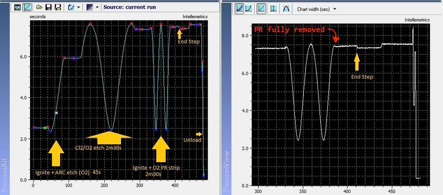
Even if you don't use the laser monitor to determine when your etched material is removed, monitoring the photoresist mask alone is very helpful. For example, you can known exactly what time the photoresist is fully etched through during an etch (even if by accident), allowing you to stop the etch at that time, and still determine selectivity if desired. |
||
[[File:ARC etch + Cr etch - UV6 at 2krpm (900nm) survived v2 - screenshot.jpg|alt=example of photoresist monitor during etch.|none|thumb|900x900px|Monitoring photoresist during two sequential etches: (1) ARC Etch (short O2 etch) |
[[File:ARC etch + Cr etch - UV6 at 2krpm (900nm) survived v2 - screenshot.jpg|alt=example of photoresist monitor during etch.|none|thumb|900x900px|Monitoring photoresist during two sequential etches: (1) ARC Etch (short O2 etch) from 100sec→120sec, and |
||
(2) subsequent Chromium etch (Cl2/O2) from 180sec until the etch completed at 500 sec. |
|||
| ⚫ | [[File:Annotated PR etch - Om1000 03 - ARC + Cl + PR etch v1.jpg|alt=annotated laser monitor plot of PR during a 3-step etch.|none|thumb|900x900px|Monitoring the photoresist during a 3-step etch. Etch (1) Etches the Anti-Reflection underlayer (BARC) |
||
Plot shows that the photoresist survived - the sinusoid continued until the etch stopped, indicating that photoresist was still present and being etched.]] |
|||
| ⚫ | |||
(2) etches Chromium with Cl2/O2 gases, and |
|||
(3) intentionally etches the photoresist quickly with O2 to remove it fully. Manually Ended the step 30 sec after the plot showed the PR was fully removed, to account for any nonuniformity across the wafer.]] |
|||
===Substrate Temperature Stabilization=== |
|||
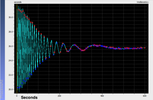
We have found that double-side polished epitaxial substrates can show an optical interference during the warm-up phase. If you see this, you need to wait until the substrate temperature has stabilized and the laser interference trace stops changing. (Thanks to [https://optoelectronics.ece.ucsb.edu/node/782 Joel Guo], [https://optoelectronics.ece.ucsb.edu/ Bowers Group]) |
|||
[[File:LaserMon - Temp Stabilize JoelGuo - 240725 noGas hold200C InPepi DSP.png|alt=laser monitor trace showing strogn oscillations gradually reducing after 8 min|none|thumb|520x520px|Double-side polished InP epitaxial piece sitting on a carrier at 200°C, strong laser traces coming from the substrate warming up. The laser trace stabilizes at around 500 sec (~8min). (Courtesy [https://optoelectronics.ece.ucsb.edu/node/782 Joel Guo], [https://optoelectronics.ece.ucsb.edu/ Bowers Group])]] |
|||
<br /> |
<br /> |
||
==References== |
==References== |
||
''See the following pages for more information about laser endpoint detection.'' |
''See the following pages for more information about laser endpoint detection.'' |
||
Latest revision as of 17:12, 26 July 2024
| ||||||||||||||||||||||
Overview
A number of our dry etching systems have Laser Etch monitors installed, for "endpoint detection". These systems allow you to end your etch at a known etch depth, or within a certain layer (with some caveats). They provide optical feedback "live" during the etch, allowing you to make the decision to terminate the etch once a target layer has been removed. This nearly eliminates the need to calibrate etch rates or to use timed etching only, which is especially important in our lab where etch rates can vary depending on the previous etches performed in the chamber.
Theory of Operation
Laser Etch monitoring works similarly to optical thin-film measurement via reflectivity spectra (eg. like our Filmetrics systems - also similar to the Woollam ellipsometer, but different technique). However, instead of varying the optical wavelength and measuring a fixed thin-film, we measure a constant wavelength and a thin-film that is getting thinner as it is etched. Thus, similar to the thin-film measurements, you can only measure a useful signal when the optical properties (reflection or interference) change during your etch. So if you can measure the start/end etch points with a Filmetrics spectrometer, then you could also use Laser Endpoint Monitor to perform the stop "live" during your etch.
For example, etching from high-reflectivity Aluminum to Lower reflectivity Silicon will usually give you a clear drop showing that your Aluminum has been fully etched-through.
Etching films that are transparent at the laser monitor wavelength (670nm on most) produces a sinusoidal signal due to optical wave interference, which gives you numerous possible stopping points to end the etch upon. See the examples below.
Limitations
Spot Size
Ideally the entire laser spot should fit inside an etched area of your wafer. The exact spot size varies on different systems based on the distance between Wafer and Laser. For the Intellemetrics systems, an open etched area of about 500 µm or larger is generally adequate to line up your laser spot. The larger the easier the alignment will be.
You also want to make sure that the laser monitor etched area is accessible to the laser on the system you are using. Please note the laser location on the dry accurate you are targeting, and to make your alignment easier, it may be beneficial to repeat the laser monitoring region on multiple die.
Layer Requirements
Because the method is based on optical interference of the incoming beam with a reflected beam, there must be some reflection of the beam by an embedded layer in order to detect an interferometric signal. Thus, the technique does not help when etching into a substrate, but only when stopping within a few microns of a layer boundary. These layer boundaries must have a refractive index difference in order to reflect the light.
The layered materials should have some transparency at the monitor wavelength of 670 nm, or exhibit a significant change in reflectivity upon etching. Layers that absorb the laser wavelength will still produce an interference signal, but only once those layers are etched thin enough to be partially transparent (eg. ~50nm for Si). You can endpoint on the removal of a metal layer, such as Al, since the reflectivity will drop significantly when the Al is fully removed.
Uniformity
Etch uniformity must still be accounted for. The laser monitor will indicate the depth at the specified laser spot, but the user must account for etch rate variations across the wafer (eg. higher etch rate at the edges of a mounted piece). Users typically will overetch past the endpoint to account for this.
Procedures
General Procedure
The basic method for performing an etch with laser monitoring endpoint, is as follows:
- Simulate or estimate what the laser monitor trace will look like, decide when to stop the etch according to the laser monitor plot.
- Mount the sample such that the laser will be able to reach a region to monitor the etch - typically ~100-300µm wide area.
- Load sample into chamber - wafer transfer only, no etch.
- Align Laser onto area to monitor using co-axial microscope.
- Start laser power monitoring/logging.
- Start Etch (time set longer than expected etch time) - etch only, no wafer transfers.
- Closely observe laser monitor plot, comparing to known/simulated plot.
- Use "Next Step" or "End Step" when appropriate laser monitor trace is reached. Wait for process to complete any final steps.
- Transfer wafer out of chamber.
- Save laser monitor data, turn off laser & microscope illumination.
Specific Procedures
Procedures for specific machines are found on the following pages:
- Intellemetrics Laser Etch Monitor Procedure - Panasonic ICP Etchers
- Installed on Panasonic ICP #1 & ICP #2
- Intellemetrics Laser Etch Monitor Procedure - Plasma-Therm Etchers
- Installed on Plasma-Therm DSE-iii and Fluorine ICP Etcher
- Intellemetrics Laser Etch Monitor - Installed on Oxford ICP Etcher
- Very similar procedure as PlasmaTherm tools. This one is an invisible 980nm nIR laser, for III-V etching.
- Horiba Laser Etch Monitor Procedure for Unaxis VLR
- Custom Laser Etch Monitor Procedure for RIE#2
- Laser Etch Monitor Procedure for RIE5
Video Training
You may self-train on the Laser Monitors with the below video. Please contact Demis for any additional questions or hands-on help.
- Video Training for Intellemetrics LEP500 Laser Etch Monitors
- Applies to Plasma-Therm Fluorine ICP (SLR) & DSE-iii, Oxford Cobra, Panasonic ICP#1 and ICP#2.
Examples
Monitoring Photoresist Etch Rate
Even if you don't use the laser monitor to determine when your etched material is removed, monitoring the photoresist mask alone is very helpful. For example, you can known exactly what time the photoresist is fully etched through during an etch (even if by accident), allowing you to stop the etch at that time, and still determine selectivity if desired.


Substrate Temperature Stabilization
We have found that double-side polished epitaxial substrates can show an optical interference during the warm-up phase. If you see this, you need to wait until the substrate temperature has stabilized and the laser interference trace stops changing. (Thanks to Joel Guo, Bowers Group)

References
See the following pages for more information about laser endpoint detection.
- Intellemetrics LEP
- The Intellemetrics Manuals are available on the tool computers in the lab - you can copy these to your Nanofiles Sync folder to access them remotely.
- Simulation of Laser Endpoint Signal in Python
