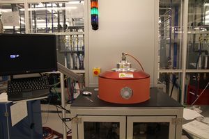
PECVD 2 (Advanced Vacuum): Difference between revisions
Jump to navigation
Jump to search
(Created page with "{{tool|{{PAGENAME}} |picture=PECVD2.jpg |type = Vacuum Deposition |super= Mike Silva |phone=(805)839-3918x219 |location=Bay 2 |email=silva@ece.ucsb.edu |description = Vision 310 …") |
(→About: alternating LS-SiN dep) |
||
| (47 intermediate revisions by 4 users not shown) | |||
| Line 1: | Line 1: | ||
{{ |
{{tool2|{{PAGENAME}} |
||
|picture=PECVD2.jpg |
|picture=PECVD2.jpg |
||
|type = Vacuum Deposition |
|type = Vacuum Deposition |
||
|super= |
|super= Michael Barreraz |
||
|super2= Don Freeborn |
|||
|phone=(805)839- |
|phone=(805)839-7975 |
||
|location=Bay 2 |
|location=Bay 2 |
||
|email=silva@ece.ucsb.edu |
|email=silva@ece.ucsb.edu |
||
|description = Vision 310 Advanced Vacuum PECVD |
|description = Vision 310 Advanced Vacuum PECVD |
||
|manufacturer = |
|manufacturer = Plasma-Therm |
||
|materials = |
|materials = |
||
|toolid=15 |
|||
}} |
}} |
||
= |
==About== |
||
This tool is designed for high quality, precise, reproducible deposition of dielectric films for optical quality films. Metallic material is ion bombarded from a target material and a reactive ion beam of oxygen and/or nitrogen is aimed at the surface, creating a metal-oxide or nitride on the sample.The system is fully computer controlled to facilitate multi-layer stack recipes for high reflectivity or low reflectivity coatings.Current available targets are Ta and Si, with Al and Ti to be added soon.The system is load locked and can handle wafers up to 6” in diameter as well as small pieces. Sample rotation and angling is used to facilitate material quality and allows for sidewall coverage on non-planar surfaces. Uniformity is better than 2% over 4" wafers and reproducibility is expected to be within one percent. |
|||
*'''Films/Gases''': This open-load system is dedicated to PECVD of '''SiO<sub>2</sub>, SiN<sub>x</sub>, SiO<sub>x</sub>N<sub>y</sub>, and a-Si''' using Silane (2%SiH<sub>4</sub>, 98% He), N<sub>2</sub>O, NH<sub>3</sub>, and N<sub>2</sub> gases. |
|||
*'''Size''': The sample electrode has a 270mm diameter useable area, allowing for multiple 4” wafer depositions in a single run. |
|||
*'''Temperature''': Standard operating temperature is 300C, but can be user changed for temps ranging anywhere from 250 to 350C. |
|||
*'''Low-Stress Si<sub>3</sub>N<sub>4</sub>''': The system is equipped with a dual generator, dual frequency option for growth of Low-stress Nitride films. |
|||
**These films alternate between thin (<10nm) compressive and tensile layers. |
|||
**The Low-Stress Si3N4 film recipe are tested approx. monthly, and kept within ±100MPa. Data can be found at Recipes (below) > [[PECVD Recipes#Historical Data 5|Low-Stress Nitride]]. |
|||
| ⚫ | |||
| ⚫ | |||
*[http://www.advanced-vacuum.se/Ny-sida-8.html Vision 310 Product Page] |
*[http://www.advanced-vacuum.se/Ny-sida-8.html Vision 310 Product Page] |
||
==Documentation== |
|||
* |
|||
* |
|||
* |
|||
* |
|||
* |
|||
* |
|||
* |
|||
* |
|||
* |
|||
* |
|||
*[https://wiki.nanotech.ucsb.edu/w/images/2/2c/SOP_for_Advanced_Vacuum_PECVD.pdf Operating Instructions] |
|||
*[[Wafer Coating Process Traveler]] |
|||
*For particle counting method, see the [[Wafer scanning process traveler|Surfscan Scanning Procedure]] |
|||
==Recipes & Historical Data== |
|||
*Recipes can be found on the PECVD Recipes Page: |
|||
**[[PECVD Recipes#PECVD 2 .28Advanced Vacuum.29|Recipes > Vacuum Deposition Recipes > PECVD Recipes > '''<u>PECVD 2 - Advanced Vacuum</u>''']] |
|||
**Thin-Films recorded: SiO2, Si3N4 and Low-Stress Si3N4 |
|||
**''Historical (Process Control) Data is also shown here.'' |
|||
*A list of ''all available'' deposited films can be found on the Vacuum Deposition Recipes page: |
|||
**[[Vacuum Deposition Recipes|Recipes > Vacuum Deposition Recipes]] |
|||
Latest revision as of 19:33, 27 August 2024
| ||||||||||||||||||||||||||||||
About
- Films/Gases: This open-load system is dedicated to PECVD of SiO2, SiNx, SiOxNy, and a-Si using Silane (2%SiH4, 98% He), N2O, NH3, and N2 gases.
- Size: The sample electrode has a 270mm diameter useable area, allowing for multiple 4” wafer depositions in a single run.
- Temperature: Standard operating temperature is 300C, but can be user changed for temps ranging anywhere from 250 to 350C.
- Low-Stress Si3N4: The system is equipped with a dual generator, dual frequency option for growth of Low-stress Nitride films.
- These films alternate between thin (<10nm) compressive and tensile layers.
- The Low-Stress Si3N4 film recipe are tested approx. monthly, and kept within ±100MPa. Data can be found at Recipes (below) > Low-Stress Nitride.
See Also
Documentation
- Operating Instructions
- Wafer Coating Process Traveler
- For particle counting method, see the Surfscan Scanning Procedure
Recipes & Historical Data
- Recipes can be found on the PECVD Recipes Page:
- Recipes > Vacuum Deposition Recipes > PECVD Recipes > PECVD 2 - Advanced Vacuum
- Thin-Films recorded: SiO2, Si3N4 and Low-Stress Si3N4
- Historical (Process Control) Data is also shown here.
- A list of all available deposited films can be found on the Vacuum Deposition Recipes page:
