PECVD 2 (Advanced Vacuum): Difference between revisions
Jump to navigation
Jump to search
Content deleted Content added
→Process Control Data: added process control images etc. |
|||
| Line 49: | Line 49: | ||
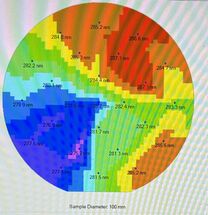
[[File:PECVD1_SiO2_F50_WaferMap_example.jpg|alt=Screenshot of Filmetrics F50 wafermap of typical DepCals film|thumb|215x215px|Example of DepCals Thickness/Refractive Index uniformity measurement (4% shown here).]] |
[[File:PECVD1_SiO2_F50_WaferMap_example.jpg|alt=Screenshot of Filmetrics F50 wafermap of typical DepCals film|thumb|215x215px|Example of DepCals Thickness/Refractive Index uniformity measurement (4% shown here).]] |
||
*Standard Recipes: [[PECVD Recipes#PECVD 2 .28Advanced Vacuum.29|'''Recipes > Deposition > <u>PECVD #2</u>''']] |
*Standard Recipes: [[PECVD Recipes#PECVD 2 .28Advanced Vacuum.29|'''Recipes > Deposition > <u>PECVD #2</u>''']] |
||
**Thin-Films recorded: SiO2, Si3N4 and Low-Stress Si3N4 |
|||
*A list of ''all available'' deposited films can be found on the Vacuum Deposition Recipes page: |
*A list of ''all available'' deposited films can be found on the Vacuum Deposition Recipes page: |
||
| Line 57: | Line 56: | ||
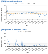
*Process Control Charts: '''[[Process Group - Process Control Data#PECVD #1 (PlasmaTherm 790) - Process Control|Process Control > PECVD#1]]''' |
*Process Control Charts: '''[[Process Group - Process Control Data#PECVD #1 (PlasmaTherm 790) - Process Control|Process Control > PECVD#1]]''' |
||
**[https://docs.google.com/spreadsheets/d/1iSW1eAAg824y9PYYLG9aiaw53PEJ-f9ofylpVlCDq9Y/edit#gid=272916741 |
**[https://docs.google.com/spreadsheets/d/1iSW1eAAg824y9PYYLG9aiaw53PEJ-f9ofylpVlCDq9Y/edit#gid=272916741 Plots of all data] |
||
**[https://docs.google.com/spreadsheets/d/1iSW1eAAg824y9PYYLG9aiaw53PEJ-f9ofylpVlCDq9Y/edit#gid=1313651154 |
**[https://docs.google.com/spreadsheets/d/1iSW1eAAg824y9PYYLG9aiaw53PEJ-f9ofylpVlCDq9Y/edit#gid=1313651154 SiO<sub>2</sub> Data] |
||
**[https://docs.google.com/spreadsheets/d/1iSW1eAAg824y9PYYLG9aiaw53PEJ-f9ofylpVlCDq9Y/edit#gid=773875841 |
**[https://docs.google.com/spreadsheets/d/1iSW1eAAg824y9PYYLG9aiaw53PEJ-f9ofylpVlCDq9Y/edit#gid=773875841 Si<sub>3</sub>N<sub>4</sub> Data] |
||
**[https://docs.google.com/spreadsheets/d/1iSW1eAAg824y9PYYLG9aiaw53PEJ-f9ofylpVlCDq9Y/edit#gid=584923738 |
**[https://docs.google.com/spreadsheets/d/1iSW1eAAg824y9PYYLG9aiaw53PEJ-f9ofylpVlCDq9Y/edit#gid=584923738 Low-Stress Si<sub>3</sub>N<sub>4</sub> Data] |
||
***[https://docs.google.com/spreadsheets/d/1iSW1eAAg824y9PYYLG9aiaw53PEJ-f9ofylpVlCDq9Y/edit#gid=203400760 Plots of Low-Stress Si<sub>3</sub>N<sub>4</sub> Data] |
***[https://docs.google.com/spreadsheets/d/1iSW1eAAg824y9PYYLG9aiaw53PEJ-f9ofylpVlCDq9Y/edit#gid=203400760 Plots of Low-Stress Si<sub>3</sub>N<sub>4</sub> Data] |
||
Revision as of 17:54, 29 September 2025
| ||||||||||||||||||||||||||||||
About
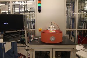
- Films/Gases: This open-load system is dedicated to PECVD of SiO2, SiNx, SiOxNy, and a-Si using Silane (2%SiH4, 98% He), N2O, NH3, and N2 gases.
- Size: The sample electrode has a 270mm diameter useable area, allowing for multiple 4” wafer depositions in a single run.
- Temperature: Standard operating temperature is 300C, but can be user changed for temps ranging anywhere from 250 to 350C.
- Low-Stress Si3N4: The system is equipped with a dual generator, dual frequency option for growth of Low-stress Nitride films.
- These films alternate between thin (<10nm) compressive and tensile layers.
- The Low-Stress Si3N4 film recipe are tested approx. monthly, and kept within ±100MPa. Data can be found at Recipes (below) > Low-Stress Nitride.
See Also
Documentation
- Operating Instructions
- Modifying Deposition Time in "STD LS-Si3N4v4" Recipe
- Modifying Deposition Temperature
- Wafer Coating Process Traveler
- For particle counting method, see the Surfscan Scanning Procedure
Recipes & Data


- Standard Recipes: Recipes > Deposition > PECVD #2
- A list of all available deposited films can be found on the Vacuum Deposition Recipes page:
Process Control Data
- Process Control Charts: Process Control > PECVD#1
