Filmetrics F40-UV Microscope-Mounted: Difference between revisions
m →About: minor text updates, curve fitting mentioned |
→Good Curve-Fitting: explained reasonable vs. perfect curve fit |
||
| (15 intermediate revisions by 3 users not shown) | |||
| Line 1: | Line 1: | ||
{{tool2 |
|||
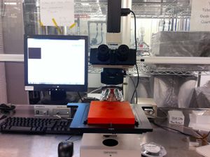
[[File:Filmetrics F40-UV - system pic 01.jpg|alt=Photograph of the system.|thumb|300x300px|Photograph of the F40-UV microsscope.]] |
|||
|super = Aidan Hopkins |
|||
|super2= Demis D. John |
|||
|picture=Filmetrics F40-UV - system pic 01.jpg |
|||
|type = Inspection, Test and Characterization |
|||
|location = Bay #4 |
|||
|description = Microscope-mounted optical reflectometry |
|||
|manufacturer = Filmetrics Inc. |
|||
|model = F40-UV |
|||
}} |
|||
== |
==About== |
||
The Filmetrics F40-UV is a microscope-mounted thin-film measurement system, allowing you to non- |
The Filmetrics F40-UV is a microscope-mounted thin-film measurement system, allowing you to non-destructively measure thin-film thicknesses in small (patterned) areas on your sample. The microscope is a standard Olympus BHJML metallurgical trinocular microscope. It is an optical reflectometer, acquiring reflection spectra between 400-900nm optical wavelengths (Vis to Near-IR) with a regular halogen microscope light source. The Filmetrics software then performs curve-fitting to determine the thickness and/or refractive index of the measured films. |
||
==Capabilities== |
|||
It is equipped with 10x, 20x, 50x, 100x and 150x objectives. |
|||
*Measure optically transparent thin-films down to ~30nm thickness. |
|||
| ⚫ | |||
*Microscope Objectives: 10x, 20x, 50x, 100x, 150x |
|||
| ⚫ | |||
**Can measure thin-films in few-micron spot. |
|||
*Acquire Optical Reflection Spectra from 400-900nm |
|||
*Spectrometer/Detector is capable of detecting down to UV ~190nm, but light source does not support this wavelength. |
|||
*Reflectivity curve-fitting for thin-film thickness analysis, supporting many common materials (Si<sub>3</sub>N<sub>4</sub>, SiO<sub>2</sub> dielectrics, Si, GaAs, InP semiconductors, metals, photoresists etc.) |
|||
*Approx ≥20nm film transparent measurement up to tens of microns. |
|||
| ⚫ | |||
| ⚫ | |||
==Examples== |
|||
===Good Curve-Fitting=== |
|||
Do not believe your thickness measurements unless the red/blue curves show a reasonably good match![[File:Filmetrics_F40-UV_-_Measurement_screenshot_on_metal_pad_01.PNG|alt=example spectrum curve fit|none|thumb|500x500px|Screenshot showing 10x microscope view and optical spectrum/curve fitting of the SiO2 film thickness on top of Platinum contact metal. This is considered a "reasonable" fit because the curves are very similar, but don't overlay perfectly, giving only reasonable confidence in the reported numbers.]] |
|||
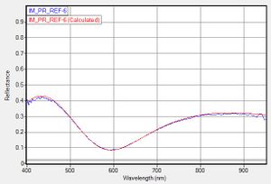
[[File:Filmetrics F40-UV - spectrum curve fit 07.jpg|alt=example spectrum curve fit|none|thumb|300x300px|A good fit should show the Calculated (red) curve overlay on top of the Measured (blue) curve. This is a very good curve-fit and the reported thickness/index should be accurate.]] |
|||
===Checking whether a dry etch is complete=== |
|||
The F40-UV is very useful for measuring whether a thin-film has been completely removed during a dry etch. This is similar to using [[Laser Etch Monitoring|laser monitoring]] during the etch, except that the microscope enables you to measure inside small patterned areas that a laser monitor spot may not fit inside. |
|||
In the following example, we are trying to etch away the SiO<sub>2</sub> from on top of a Platinum contact metal. The 20x objective allows us to measure the SiO2 thickness on top of the Platinum as we continue to etch in 1 minute increments, measuring in between etches. |
|||
Finally, when the SiO2 has been fully removed, we see that we can't get a good fit between the measured (blue) and simulated (red) data. |
|||
Since the Platinum layer is thick enough to be opaque to visible light (>50nm), we just modelled this as SiO2 on top of Platinum, ignoring any other materials below the platinum. |
|||
{| class="wikitable" |
|||
|+ |
|||
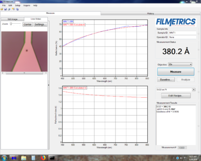
![[File:Filmetrics F40-UV - SiO Etch 4m+4m - Incomplete Etch.png|alt=Example Screenshot of incomplete SiO2 etch|none|thumb|400x400px|Incomplete Dry-Etch, showing some residual SiO2 left. "Goodness of Fit" is close to 1.0 in the results pane, and the red+blue curves match closely so we believe the measurement.]] |
|||
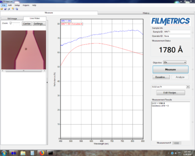
![[File:Filmetrics F40-UV - 2018-11-08 - SiO Etch 4m+4m+1m - Fully Removed.png|alt=Example screenshot of fully removed SiO2 etch|none|thumb|400x400px|After re-etching, measurement shows bad fit (red and blue curves), and "Goodness of Fit" = 0 in the results pane. |
|||
The thickness value shown is not real, and this indicates that the SiO2 film has been fully removed since no parameter can give a good fit. |
|||
]] |
|||
|} |
|||
==Other Info== |
|||
'''''Equip > Characterization > <u>[[Microscopes]]</u>''''' - ''see a list of all our microscopes'' |
|||
Latest revision as of 21:28, 29 September 2022
| ||||||||||||||||||||||||||||
About
The Filmetrics F40-UV is a microscope-mounted thin-film measurement system, allowing you to non-destructively measure thin-film thicknesses in small (patterned) areas on your sample. The microscope is a standard Olympus BHJML metallurgical trinocular microscope. It is an optical reflectometer, acquiring reflection spectra between 400-900nm optical wavelengths (Vis to Near-IR) with a regular halogen microscope light source. The Filmetrics software then performs curve-fitting to determine the thickness and/or refractive index of the measured films.
Capabilities
- Measure optically transparent thin-films down to ~30nm thickness.
- Microscope Objectives: 10x, 20x, 50x, 100x, 150x
- Can measure thin-films in few-micron spot.
- Acquire Optical Reflection Spectra from 400-900nm
- Spectrometer/Detector is capable of detecting down to UV ~190nm, but light source does not support this wavelength.
- Reflectivity curve-fitting for thin-film thickness analysis, supporting many common materials (Si3N4, SiO2 dielectrics, Si, GaAs, InP semiconductors, metals, photoresists etc.)
- Approx ≥20nm film transparent measurement up to tens of microns.
Operating Procedures
Examples
Good Curve-Fitting
Do not believe your thickness measurements unless the red/blue curves show a reasonably good match!


Checking whether a dry etch is complete
The F40-UV is very useful for measuring whether a thin-film has been completely removed during a dry etch. This is similar to using laser monitoring during the etch, except that the microscope enables you to measure inside small patterned areas that a laser monitor spot may not fit inside.
In the following example, we are trying to etch away the SiO2 from on top of a Platinum contact metal. The 20x objective allows us to measure the SiO2 thickness on top of the Platinum as we continue to etch in 1 minute increments, measuring in between etches.
Finally, when the SiO2 has been fully removed, we see that we can't get a good fit between the measured (blue) and simulated (red) data.
Since the Platinum layer is thick enough to be opaque to visible light (>50nm), we just modelled this as SiO2 on top of Platinum, ignoring any other materials below the platinum.
Other Info
Equip > Characterization > Microscopes - see a list of all our microscopes


