ICP-PECVD (Unaxis VLR): Difference between revisions
added cluster configuration / link to each chamber's tool page |
added Process Control Data section |
||
| (41 intermediate revisions by 4 users not shown) | |||
| Line 1: | Line 1: | ||
{{ |
{{tool2|{{PAGENAME}} |
||
|picture=UnaxisPECVD.jpg |
|picture=UnaxisPECVD.jpg |
||
|type = Vacuum Deposition |
|type = Vacuum Deposition |
||
|super= Tony Bosch |
|super= Tony Bosch |
||
|super2= Don Freeborn |
|||
|phone=(805)839-3918x217 |
|phone=(805)839-3918x217 |
||
|location=Bay 1 |
|location=Bay 1 |
||
| Line 12: | Line 13: | ||
}} |
}} |
||
=About= |
=About= |
||
This system is configured as an ICP PECVD deposition tool with 1000 W ICP power, 600 W RF substrate power, and |
This system is configured as an ICP PECVD deposition tool with 1000 W ICP power, 600 W RF substrate power, and 100°C-350°C operation. This chamber has 100% SiD<sub>4,</sub> N<sub>2</sub>, O<sub>2</sub>, and Ar for gas sources. The high density PECVD produces a more dense, higher quality SiO<sub>2</sub> and Si<sub>3</sub>N<sub>4</sub>, as compared with conventional PECVD. With the high density plasma, deposition of high quality films can be deposited as low as 100°C for processes requiring lower temperatures. Stress compensation for silicon nitride is characterized. Processes are available for Gap-filling with SiO<sub>2</sub>. |
||
=== |
===Cluster Configuration=== |
||
A Deposition and Etch chamber are both attached to the same loadlock, allowing etching and deposition without breaking vacuum. Each chamber can be scheduled separately on SignupMonkey. |
A Deposition and Etch chamber are both attached to the same loadlock, allowing etching and deposition without breaking vacuum. Each chamber can be scheduled separately on SignupMonkey. |
||
* |
*'''PM3''': ICP-PECVD Deposition (this page) |
||
* |
*'''PM1''': [[ICP-Etch (Unaxis VLR)|ICP Etch (Unaxis VLR)]] |
||
=Detailed Specifications= |
=Detailed Specifications= |
||
*1000W ICP source, 600W RF Sample Bias Power Supply |
*1000W ICP source, 600W RF Sample Bias Power Supply |
||
* |
*100 - 350°C sample temperature |
||
*100% |
*100% SiD<sub>4</sub>, Ar, N<sub>2</sub>, O<sub>2</sub> |
||
*Multiple 4” diameter wafer capable system |
*Multiple 4” diameter wafer capable system |
||
*Pieces possible by mounting or placing on 4 ” wafer |
*Pieces possible by mounting or placing on 4 ” wafer |
||
The Deposition chamber currently has '''Deuterated Silane (SiD<sub>4</sub>)''' installed - identical to the normal Silicon precursor SiH<sub>4</sub>, except that it significantly lowers optical absorption in the near-infrared. This gas is '''expensive''' and thus more applicable to optical applications than to general-purpose SiN films. |
|||
=Documentation= |
=Documentation= |
||
*[ |
*[[Unaxis VLR ICP-PECVD - Std. Operating Procedure|Operating Instructions]] |
||
*[[Unaxis wafer coating procedure]] - ''process flow for achieving high-quality coatings.'' |
|||
**For particle counting procedure, see the [https://wiki.nanotech.ucsb.edu/wiki/Wafer_scanning_process_traveler Surfscan Scanning Procedure] |
|||
*Online Training Video: |
|||
**[https://gauchocast.hosted.panopto.com/Panopto/Pages/Viewer.aspx?id=1af6f3ce-8fc4-4a50-884a-ae3600d2863d <u>Unaxis ICP-PECVD Training</u>] |
|||
**'''Important:''' ''This video is for reference only, and does not give you authorization to use the tool. You must be officially authorized by the supervisor before using this machine.'' |
|||
You must log in using your UCSB ID Net account information BEFORE viewing the video or you will have to watch the video again. |
|||
==Recipes== |
|||
You can find recipes for this tool on the '''Wiki > Recipes >''' [https://wiki.nanotech.ucsb.edu/wiki/PECVD_Recipes#ICP-PECVD_.28Unaxis_VLR.29 '''<u>PECVD Recipes page</u>'''] |
|||
== Process Control Data == |
|||
You can see calibration data for the thin-films on this tool at the '''Recipes >''' [[PECVD Recipes#Process Control Data .28Unaxis ICP-PECVD.29|'''<u>Process Control Data page</u>''']]. |
|||
Latest revision as of 17:35, 23 May 2023
| ||||||||||||||||||||||||||||||
About
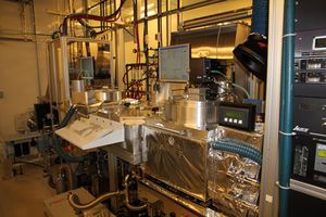
This system is configured as an ICP PECVD deposition tool with 1000 W ICP power, 600 W RF substrate power, and 100°C-350°C operation. This chamber has 100% SiD4, N2, O2, and Ar for gas sources. The high density PECVD produces a more dense, higher quality SiO2 and Si3N4, as compared with conventional PECVD. With the high density plasma, deposition of high quality films can be deposited as low as 100°C for processes requiring lower temperatures. Stress compensation for silicon nitride is characterized. Processes are available for Gap-filling with SiO2.
Cluster Configuration
A Deposition and Etch chamber are both attached to the same loadlock, allowing etching and deposition without breaking vacuum. Each chamber can be scheduled separately on SignupMonkey.
- PM3: ICP-PECVD Deposition (this page)
- PM1: ICP Etch (Unaxis VLR)
Detailed Specifications
- 1000W ICP source, 600W RF Sample Bias Power Supply
- 100 - 350°C sample temperature
- 100% SiD4, Ar, N2, O2
- Multiple 4” diameter wafer capable system
- Pieces possible by mounting or placing on 4 ” wafer
The Deposition chamber currently has Deuterated Silane (SiD4) installed - identical to the normal Silicon precursor SiH4, except that it significantly lowers optical absorption in the near-infrared. This gas is expensive and thus more applicable to optical applications than to general-purpose SiN films.
Documentation
- Operating Instructions
- Unaxis wafer coating procedure - process flow for achieving high-quality coatings.
- For particle counting procedure, see the Surfscan Scanning Procedure
- Online Training Video:
- Unaxis ICP-PECVD Training
- Important: This video is for reference only, and does not give you authorization to use the tool. You must be officially authorized by the supervisor before using this machine.
You must log in using your UCSB ID Net account information BEFORE viewing the video or you will have to watch the video again.
Recipes
You can find recipes for this tool on the Wiki > Recipes > PECVD Recipes page
Process Control Data
You can see calibration data for the thin-films on this tool at the Recipes > Process Control Data page.
