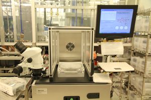
XeF2 Etch (Xetch): Difference between revisions
No edit summary |
Millerski w (talk | contribs) Updated SOP |
||
| (5 intermediate revisions by 3 users not shown) | |||
| Line 1: | Line 1: | ||
{{ |
{{tool2|{{PAGENAME}} |
||
|picture=XeF2.jpg |
|picture=XeF2.jpg |
||
|type = Dry Etch |
|type = Dry Etch |
||
|super= Bill Millerski |
|super= Bill Millerski |
||
|super2= Don Freeborn |
|||
|phone=(805)839-3918x216 |
|phone=(805)839-3918x216 |
||
|location=Bay 2 |
|location=Bay 2 |
||
| Line 11: | Line 12: | ||
|toolid=31 |
|toolid=31 |
||
}} |
}} |
||
= |
==About== |
||
The applications of this tool are mainly in MEMS-device fabrication areas (releasing a MEMS structure by etching a sacrificial layer below), in which Si or Ge or even some metals, such as Mo, can be isotropically dry etched using gaseous XeF<sub>2</sub> (no plasma enhancement or heating is needed) with the use of photoresist or SiO<sub>2</sub> or Al as an etch mask at room temperature. |
The applications of this tool are mainly in MEMS-device fabrication areas (releasing a MEMS structure by etching a sacrificial layer below), in which Si or Ge or even some metals, such as Mo, can be isotropically dry etched using gaseous XeF<sub>2</sub> (no plasma enhancement or heating is needed) with the use of photoresist or SiO<sub>2</sub> or Al as an etch mask at room temperature. |
||
| Line 22: | Line 23: | ||
For users who want to etch through or very deep into a Si wafer, they should use the Si Deep RIE tool in the lab. |
For users who want to etch through or very deep into a Si wafer, they should use the Si Deep RIE tool in the lab. |
||
=Documentation= |
==Documentation== |
||
*[//wiki.nanotech.ucsb.edu/w/images/7/7b/Xactic-XetchX3-System-Manual.pdf System Manual] |
*[//wiki.nanotech.ucsb.edu/w/images/7/7b/Xactic-XetchX3-System-Manual.pdf System Manual] |
||
*[//wiki.nanotech.ucsb.edu/w/images/c/c0/XeF2-Results.pdf Si Etching Profile & Results] |
*[//wiki.nanotech.ucsb.edu/w/images/c/c0/XeF2-Results.pdf Si Etching Profile & Results] |
||
*{{file|XACTI XeF2 Etch Operating Instructions.pdf|XACTI XeF2 etch |
*{{file|XACTI XeF2 Etch Operating Instructions.pdf|XACTI XeF2 etch Instructions}} |
||
==Operation Procedure== |
|||
*[https://wiki.nanofab.ucsb.edu/w/images/1/10/XeF2_Etch_Operating_Instructions.pdf XeF2 Etch Operating Procedure] |
|||
==Recipes== |
|||
*[[Other Dry Etching Recipes#XeF2%20Etch%20.28Xetch.29|Other Dry Etching Recipes: XeF2 Etcher]] |
|||
Latest revision as of 22:03, 30 October 2023
| ||||||||||||||||||||||||||||||
About
The applications of this tool are mainly in MEMS-device fabrication areas (releasing a MEMS structure by etching a sacrificial layer below), in which Si or Ge or even some metals, such as Mo, can be isotropically dry etched using gaseous XeF2 (no plasma enhancement or heating is needed) with the use of photoresist or SiO2 or Al as an etch mask at room temperature.
The XeF2 etch process is a purely chemical one and usually results in a rough etched surface. The tool is operated in a pulsed mode in which the etch chamber is repeatedly filled with XeF2 gas and, then, pumped out (to 0.3 Torr). You can also add N2 gas, together with XeF2 gas, into the etch chamber for some applications.
There is a microscope attached to this tool, with which you can monitor the etch process of your sample. You can change the number of etch cycles during a run, which will be effective in that run. Also, you can manually stop a run based on microscope observations.
Maximum Wafer size is 6".
For users who want to etch through or very deep into a Si wafer, they should use the Si Deep RIE tool in the lab.
