ICP Etch 1 (Panasonic E646V): Difference between revisions
separate process control section/link |
added "tool down, use ICP2" note |
||
| (9 intermediate revisions by 3 users not shown) | |||
| Line 1: | Line 1: | ||
'''<big>2025-09: This tool is currently inoperable due to unrecoverable hardware failures! Please use [[ICP Etch 2 (Panasonic E626I)|<u>Panasonic ICP #2</u>]] instead, nearly a direct replacement.</big>''' |
|||
{{ |
{{tool2|{{PAGENAME}} |
||
|picture=ICP2.jpg |
|picture=ICP2.jpg |
||
|type = Dry Etch |
|type = Dry Etch |
||
|super= Lee Sawyer |
|super= Lee Sawyer |
||
|super2= Don Freeborn |
|||
|location=Bay 2 |
|location=Bay 2 |
||
|description = ICP Etching and Ashing Multi-Chamber Tool |
|description = ICP Etching and Ashing Multi-Chamber Tool |
||
|manufacturer = Panasonic Factory Solutions, Japan |
|manufacturer = Panasonic Factory Solutions, Japan |
||
|model=E646V |
|||
|materials = |
|materials = |
||
|toolid=22 |
|toolid=22 |
||
}} |
}} |
||
__TOC__ |
|||
==About== |
==About== |
||
| Line 57: | Line 63: | ||
*[https://wiki.nanotech.ucsb.edu/w/images/0/0a/ICP_-1_Gas_Change_CF4-SF6-CF4.pdf]{{file|Panasonic 1 instructions.pdf|Panasonic _1_instructions.pdf}} |
*[https://wiki.nanotech.ucsb.edu/w/images/0/0a/ICP_-1_Gas_Change_CF4-SF6-CF4.pdf]{{file|Panasonic 1 instructions.pdf|Panasonic _1_instructions.pdf}} |
||
*[https://wiki.nanotech.ucsb.edu/w/images/0/0a/ICP_-1_Gas_Change_CF4-SF6-CF4.pdf ICP #1 Gas Change Procedure: CF<sub>4</sub>-SF<sub>6</sub>-CF<sub>4</sub>] |
*[https://wiki.nanotech.ucsb.edu/w/images/0/0a/ICP_-1_Gas_Change_CF4-SF6-CF4.pdf ICP #1 Gas Change Procedure: CF<sub>4</sub>-SF<sub>6</sub>-CF<sub>4</sub>] |
||
*[https://wiki.nanotech.ucsb.edu/w/images/ |
*[https://wiki.nanotech.ucsb.edu/w/images/8/8c/ICP_-1_Gas_Change_CHF3-Ar.pdf ICP #1 Gas Change Procedure: CHF<sub>3</sub>-Ar-CHF<sub>3</sub>] |
||
*[https://wiki.nanotech.ucsb.edu/w/images/f/fa/ICP_-1_Gas_Change_N2-He-N2.pdf ICP #1 Gas Change Procedure: N<sub>2</sub>-He-N<sub>2</sub>] |
*[https://wiki.nanotech.ucsb.edu/w/images/f/fa/ICP_-1_Gas_Change_N2-He-N2.pdf ICP #1 Gas Change Procedure: N<sub>2</sub>-He-N<sub>2</sub>] |
||
*[https://wiki.nanotech.ucsb.edu/w/images/3/3a/ICP_-1_Rules_%26_Important_Notes.pdf ICP #1 Rules and Important Notes] |
*[https://wiki.nanotech.ucsb.edu/w/images/3/3a/ICP_-1_Rules_%26_Important_Notes.pdf ICP #1 Rules and Important Notes] |
||
*[https://wiki.nanofab.ucsb.edu/w/images/4/48/ICP_-1_Standard_Etch_Recipes.pdf ICP #1 Standard Recipes] |
|||
*[https://wiki.nanotech.ucsb.edu/w/images/d/de/ICP_-1_Wafer_Type_Change.pdf ICP #1 Wafer Type Change Procedure] |
|||
*[[Laser Etch Monitoring|Laser Etch Monitor procedures]] |
*[[Laser Etch Monitoring|Laser Etch Monitor procedures]] |
||
Latest revision as of 01:38, 27 November 2025
2025-09: This tool is currently inoperable due to unrecoverable hardware failures! Please use Panasonic ICP #2 instead, nearly a direct replacement.
| ||||||||||||||||||||||||||||||||
About
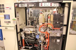
This is a three-chamber tool for etching of a variety of materials.
Chamber one "Etch Chamber" is configured as an ICP etching tool with 1000 W ICP power, 500 W RF substrate power, and RT - 80°C operation with back-side He cooling and an electrostatic chuck to maintain controlled surface temperatures during etching.
This chamber has the following dedicated gas sources: Cl2, BCl3, and O2
The chamber also has the following gas sources, where two of the lines must be manually switched between the two options shown (gasses can't be used simultaneously): N2/He, CHF3/Ar and CF4 /SF6
The system can be used to etch a variety of materials from SiO2 to metals to compound semiconductors. The chamber is evacuated with a 2000 lpm Osaka Vacuum magnetically levitated turbo pump, and is load-locked for fast pump down.
The in-situ laser monitor installed on the etch chamber allows for repeatable etches and endpoint detection via continuous optical monitoring of the wafer reflectivity in a user-determined location, through a porthole on the chamber.
Chamber two, "Ashing Chamber" is a 2000 W ICP chamber configures for plasma "ashing" of photoresist and other materials such as BCB. The substrate is not biased for isotropic etching, and the chamber has CF4 and O2 for the gases. This is especially well-suited for omni-directional etching of photoresist/PR removal, or BCB etch-back.
Chamber three "Rinse Chamber" is a DI rinsing chamber that is not used/offline.
The system accepts 6” wafers with SEMI-std. flats. Users often mount smaller pieces to the wafers, usually with easily removable oil to improve uniform heat-sinking.
In Automatic mode, multiple wafers can be run through automatically with the cassette-based system.
Detailed Specifications
- 1000 W ICP source, 500 W RF Sample Bias Source in etching chamber
- Multiple 6” diameter wafer capable system
- Pieces possible by mounting to 6” wafer
Etch Chamber:
- Optimal Emission Monitoring
- Etch pressure from 0.1 Pa to 5 Pa (0.75 mT - 37.5 mT)
- Cl2, BCl3, O2, (CHF3 or Ar), (CF4 or SF6), and (N2 or He) in etch chamber
- Room Temp - 80°C sample temperature for etching. Default 12°C Chuck Temperature.
- Laser Etch Monitoring: Intellemetrics LEP 500
Ashing Chamber:
- 2000 W ICP ashing chamber
- RT - 250°C sample temperature for ashing
- Ashing pressures 50 mT - 500 mT
- O2, N2, CF4, H2O Vapor for ashing chamber
- Room Temp. to 270°C etching. Default 50°C.
Documentation
- [1]Panasonic _1_instructions.pdf
- ICP #1 Gas Change Procedure: CF4-SF6-CF4
- ICP #1 Gas Change Procedure: CHF3-Ar-CHF3
- ICP #1 Gas Change Procedure: N2-He-N2
- ICP #1 Rules and Important Notes
- ICP #1 Standard Recipes
- ICP #1 Wafer Type Change Procedure
- Laser Etch Monitor procedures
Recipes
- Recipes > Dry Etching > ICP Etch 1 page lists all qualified and contributed recipes for this tool.
- Starting point recipes for ICP#1
- Process Control Data
- Historical Data records "calibration" etches to test tool performance.
- The Recipes > Dry Etching Recipes
- Master table lists all contributed dry etches vs etched materials across tools.
