PECVD 1 (PlasmaTherm 790): Difference between revisions
| (65 intermediate revisions by 8 users not shown) | |||
| Line 1: | Line 1: | ||
{{ |
{{tool2|{{PAGENAME}} |
||
|picture=PECVD1.jpg |
|picture=PECVD1.jpg |
||
|type = Vacuum Deposition |
|type = Vacuum Deposition |
||
|super= |
|super= Michael Barreraz |
||
|super2= Don Freeborn |
|||
|phone=(805)839- |
|phone=(805)839-7975 |
||
|location=Bay 3 |
|location=Bay 3 |
||
|email= |
|email=dfreeborn@ucsb.edu |
||
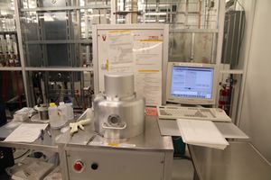
|description = PECVD Plasma Therm 790 For Oxides And Nitrides |
|description = PECVD Plasma Therm 790 For Oxides And Nitrides |
||
|manufacturer = Plasma-Therm |
|manufacturer = Plasma-Therm |
||
|materials = |
|materials = |
||
|toolid=16 |
|||
| ⚫ | |||
}} |
|||
| ⚫ | |||
= About = |
== About == |
||
'''Films:''' This is a Plasma-Therm model 790 plasma enhanced chemical vapor deposition system for depositing SiO<sub>2</sub>, Si<sub>3</sub>N<sub>4</sub>, or SiO<sub>x</sub>N<sub>y</sub> dielectric films. |
|||
This is a Plasma-Therm model 790 plasma enhanced chemical vapor deposition system for depositing SiO<sub>2</sub>, Si<sub>3</sub>N<sub>4</sub>, or SiO<sub>x</sub>N<sub>y</sub> dielectric films. The system uses a capacitively-coupled 13.56 MHz source excitation to produce the plasma between two parallel aluminum plates. The gas is injected over the sample through a 6” diameter showerhead. The samples are placed on the system anode (to minimize ion damage) which is heated to 250-350°C. SiO<sub>2</sub> is produced from SiH<sub>4</sub>/He 2%/98% and N<sub>2</sub>O at 250°C. The typical deposition rate is 400 A/min. at 300 mT pressure. The typical BOE etch rate of this oxide is about 400 nm/min. Si<sub>3</sub>N<sub>4</sub> is produced from SiH<sub>4</sub>/He 2%/98% and NH<sub>3</sub> at 250°C or 350°C. The more dense films are produced at 350°C. The stress of the nitride can be altered by adjusting the N<sub>2</sub>:He ratio of the deposition. CF<sub>4</sub>/O<sub>2</sub> plasmas are used to clean the chamber between depositions. |
|||
'''Hardware:''' The system uses a capacitively-coupled 13.56 MHz source excitation to produce the plasma between two parallel aluminum plates. The gas is injected over the sample through a 6” diameter showerhead. The samples are placed on the system anode (to minimize ion damage) which is heated to 250-350°C (250°C is standard). |
|||
These films are typically used for capacitor dielectrics, chemical passivation layers, electrical insulators, reactive ion etching masks, and optical anti-reflective coatings. The system is fully programmable with windows-based software and has a wide array of pre-defined thicknesses. Custom programs for dielectric stacks or different process parameters can be written and saved. |
|||
'''Gases:''' |
|||
| ⚫ | |||
SiH<sub>4</sub> (Silane) is the Silicon precursor gas. It is diluted with He down to 2% Silane for safety. |
|||
| ⚫ | |||
| ⚫ | |||
N<sub>2</sub>O is the Oxygen precursor gas, for producing SiO<sub>2</sub>. |
|||
| ⚫ | |||
NH<sub>4</sub> is the Nitrogen precursor gas, for producing Si<sub>3</sub>N<sub>4</sub>. |
|||
CF<sub>4</sub> & O<sub>2</sub> are used for plasma-cleaning the chamber, by etching off deposited SiO<sub>2</sub>/Si<sub>3</sub>N<sub>4</sub> films from the chamber walls (in addition to wet-cleaning the chamber walls). |
|||
N<sub>2</sub> is available as a purging gas or carrier gas. A very low percentage of N<sub>2</sub> is expected to "crack" at the low RF powers used on this system. |
|||
'''Film Properties:''' |
|||
SiO<sub>2</sub> is produced from SiH<sub>4</sub>/He 2%/98% and N<sub>2</sub>O at 250°C. The typical deposition rate is 400 Å/min at 300 mT pressure. The typical BOE etch rate of this oxide is about 400 nm/min. |
|||
Si<sub>3</sub>N<sub>4</sub> is produced from SiH<sub>4</sub>/He 2%/98% and NH<sub>3</sub> at 250°C or 350°C. The more dense films are produced at 350°C. The stress of the nitride can be altered by adjusting the N<sub>2</sub>:He ratio of the deposition. |
|||
'''Applications:''' These films are typically used for reactive ion etching masks, electrical insulators, chemical passivation layers, optical anti-reflective coatings and capacitor dielectrics. The system is fully programmable with windows-based software. |
|||
'''Usage:''' Users type in a deposition time for each recipe, using the published (or user-measured) deposition rates. Current dep rates for standard films can be found on [[Process Group - Process Control Data#PECVD #1 (PlasmaTherm 790) - Process Control|the PECVD#1 process control data charts]]. |
|||
Custom programs for dielectric stacks or different process parameters or SiO<sub>x</sub>N<sub>y</sub> films can be written and saved. |
|||
| ⚫ | |||
| ⚫ | |||
| ⚫ | |||
| ⚫ | |||
| ⚫ | |||
| ⚫ | |||
*Sample size: pieces to 6” wafers |
*Sample size: pieces to 6” wafers |
||
| ⚫ | |||
| ⚫ | |||
*Full computer operation |
*Full computer operation |
||
*Standard recipes |
*Standard recipes with deposition variable time |
||
==Documentation== |
|||
*[https://wiki.nanofab.ucsb.edu/w/images/6/64/IMG_7361.jpg Operating Instructions] |
|||
*[[PECVD1 Wafer Coating Process|Wafer Coating Process Traveler]] |
|||
*For particle counting method, see the [https://wiki.nanotech.ucsb.edu/wiki/Wafer_scanning_process_traveler Surfscan Scanning Procedure] |
|||
== Recipes & Data == |
|||
* Standard Recipes: [[PECVD Recipes#PECVD 1 .28PlasmaTherm 790.29|'''Recipes > Deposition > <u>PECVD#1</u>''']] |
|||
** A list of ''all available'' deposited films can be found here: [[Vacuum Deposition Recipes|Recipes > Vacuum Deposition Recipes]] |
|||
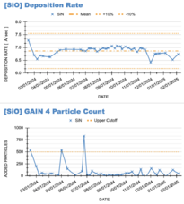
* Process Control Charts: '''[[Process Group - Process Control Data#PECVD #1 (PlasmaTherm 790) - Process Control|Process Control > PECVD#1]]''' |
|||
[[File:PECVD SPC Chart Example.png|alt=SPC chart example|thumb|228x228px|Example Process Control Charts (SPC) for thin-film DepCals.|none]] |
|||
[[File:Surfscan 230113A7G2 after low particles.jpg|alt=screenshot of surfscan particle count|thumb|205x205px|Example particle counts taken on each film.|none]] |
|||
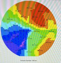
[[File:PECVD1 SiO2 F50 WaferMap example.jpg|alt=Screenshot of Filmetrics F50 wafermap of typical DepCals film|thumb|215x215px|Example of DepCals Thickness/Refractive Index uniformity measurement (4% shown here).|none]] |
|||
Latest revision as of 17:55, 29 September 2025
| ||||||||||||||||||||||||||||||
About
Films: This is a Plasma-Therm model 790 plasma enhanced chemical vapor deposition system for depositing SiO2, Si3N4, or SiOxNy dielectric films.
Hardware: The system uses a capacitively-coupled 13.56 MHz source excitation to produce the plasma between two parallel aluminum plates. The gas is injected over the sample through a 6” diameter showerhead. The samples are placed on the system anode (to minimize ion damage) which is heated to 250-350°C (250°C is standard).
Gases:
SiH4 (Silane) is the Silicon precursor gas. It is diluted with He down to 2% Silane for safety.
N2O is the Oxygen precursor gas, for producing SiO2.
NH4 is the Nitrogen precursor gas, for producing Si3N4.
CF4 & O2 are used for plasma-cleaning the chamber, by etching off deposited SiO2/Si3N4 films from the chamber walls (in addition to wet-cleaning the chamber walls).
N2 is available as a purging gas or carrier gas. A very low percentage of N2 is expected to "crack" at the low RF powers used on this system.
Film Properties:
SiO2 is produced from SiH4/He 2%/98% and N2O at 250°C. The typical deposition rate is 400 Å/min at 300 mT pressure. The typical BOE etch rate of this oxide is about 400 nm/min.
Si3N4 is produced from SiH4/He 2%/98% and NH3 at 250°C or 350°C. The more dense films are produced at 350°C. The stress of the nitride can be altered by adjusting the N2:He ratio of the deposition.
Applications: These films are typically used for reactive ion etching masks, electrical insulators, chemical passivation layers, optical anti-reflective coatings and capacitor dielectrics. The system is fully programmable with windows-based software.
Usage: Users type in a deposition time for each recipe, using the published (or user-measured) deposition rates. Current dep rates for standard films can be found on the PECVD#1 process control data charts.
Custom programs for dielectric stacks or different process parameters or SiOxNy films can be written and saved.
Detailed Specifications
- Gases available: NH3, N2O, 2%SiH4/He, N2,CF4 and O2
- ~10mT base chamber pressure
- 13.56 MHz excitation freq.
- Automatic tuning network
- RF Power control
- Sample size: pieces to 6” wafers
- Full computer operation
- Standard recipes with deposition variable time
Documentation
- Operating Instructions
- Wafer Coating Process Traveler
- For particle counting method, see the Surfscan Scanning Procedure
Recipes & Data
- Standard Recipes: Recipes > Deposition > PECVD#1
- A list of all available deposited films can be found here: Recipes > Vacuum Deposition Recipes
- Process Control Charts: Process Control > PECVD#1


