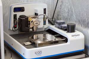
Atomic Force Microscope (Bruker ICON): Difference between revisions
Created page with "{{tool|{{PAGENAME}} |picture=AFMNanoman.jpg |type = Lithography |super= Bill Mitchell |phone= (805)893-4974 |location=Bay 7 |email=mitchell@ece.ucsb.edu |description = Dimension …" |
No edit summary |
||
| (16 intermediate revisions by 2 users not shown) | |||
| Line 1: | Line 1: | ||
{{ |
{{tool2|{{PAGENAME}} |
||
|picture= |
|picture=ICON_AFM.jpg |
||
|type = Inspection, Test and Characterization |
|||
|type = Lithography |
|||
|super= |
|super= Aidan Hopkins |
||
|super2= Bill Mitchell |
|||
|phone= (805)893-4974 |
|phone= (805)893-4974 |
||
|location=Bay |
|location=Bay 5 |
||
|email=mitchell@ece.ucsb.edu |
|email=mitchell@ece.ucsb.edu |
||
|description = |
|description = Bruker ICON AFM |
||
|manufacturer = |
|manufacturer = Bruker Nano, Inc |
||
|materials = |
|materials = |
||
|toolid= 1 |
|||
}} |
}} |
||
= About = |
= About = |
||
The Bruker ICON AFM utilizes the latest paradigm in Atomic Force Microscopy - '''PeakForce Tapping®,''' a method that combines the best features of the legacy Contact Mode and Tapping Mode imaging techniques, namely direct force control and intermittent surface contact to reduce damaging lateral forces, to precisely control the probe-to-surface force interaction as pixel-to-pixel force curve measurements. This control results in the most consistent, highest resolution AFM imaging technique that can be used on a wide range of sample types. |
|||
The Dimension 3100 Nanoman AFM from Veeco provides a variety of high resolution surface imaging techniques and the ability to manipulate or create nanoscale structures directly. Techniques available for imaging include contact mode AFM, tapping mode AFM, Scanning Tunnelling AFM, Conductive AFM, and Scanning Capacitance Microscopy. With the Nanoman option, the X and Y deflecting piezo-elements are independently controlled, allowing for precise and direct placement of the tip anywhere within the field. Direct manipulation of particles on the surface is then possible by dragging the tip in the desired direction. This feedback control, coupled with direct control of conductive tip and substrate voltages, allows for direct-write oxidation on a variety of surfaces to create or modify nanostructures through local anodization. |
|||
Note that the ICON AFM also can also utilize the legacy ContactMode and TappingMode techniques for imaging if required. |
|||
In PeakForce Tapping®, the probe periodically taps the sample and the pN-level interaction force is measured directly by the deflection of the cantilever. Through superior force control, the feedback loop keeps the peak force constant, down to pN range, in both air and fluid, which is significantly lower than is typically used with other modes, such as TappingMode™, in the 1-10 nN range. PeakForce Tapping® enables the researcher to precisely control probe-to-sample interaction, providing the lowest available imaging forces. |
|||
=Detailed Specifications= |
=Detailed Specifications= |
||
*PeakForce Tapping® imaging for superior resolution and consistency |
|||
*Conductive AFM modules for nA-microAmp current measurements |
|||
*Legacy Contact Mode and Tapping Mode imaging also available |
|||
*Tunneling AFM modulefor pA-nA current measurements |
|||
*Substrate size range: small pieces (>2mm) up to 4" wafers |
|||
| ⚫ | |||
*Computer controlled XY stage for superior sample positioning; piezo Z scan range ~ 12um |
|||
*Resolution: Sub-nm height-measurement capability; X-Y resolution tip dependent |
|||
*Basic electrical measurement techniques are available but only using Contact Mode imaging. |
|||
*Registration tolerance to a known mark: Field size dependent |
|||
| ⚫ | |||
*Minimum substrate size: small pieces |
|||
**Conductive AFM (CAFM) for high currents, Tunneling AFM (TUNA) for low currents |
|||
*Largest substrate size: 100 mm wafer |
|||
*Oxidation Line widths: Call for info. |
|||
=See Also= |
=See Also= |
||
*[https://www.bruker.com/products/surface-and-dimensional-analysis/atomic-force-microscopes/dimension-icon/overview.html Bruker ICON AFM overview] |
|||
*[http://www.veeco.com/ Veeco Website] |
|||
Latest revision as of 18:57, 30 August 2022
| ||||||||||||||||||||||||||||||
About
The Bruker ICON AFM utilizes the latest paradigm in Atomic Force Microscopy - PeakForce Tapping®, a method that combines the best features of the legacy Contact Mode and Tapping Mode imaging techniques, namely direct force control and intermittent surface contact to reduce damaging lateral forces, to precisely control the probe-to-surface force interaction as pixel-to-pixel force curve measurements. This control results in the most consistent, highest resolution AFM imaging technique that can be used on a wide range of sample types.
Note that the ICON AFM also can also utilize the legacy ContactMode and TappingMode techniques for imaging if required.
In PeakForce Tapping®, the probe periodically taps the sample and the pN-level interaction force is measured directly by the deflection of the cantilever. Through superior force control, the feedback loop keeps the peak force constant, down to pN range, in both air and fluid, which is significantly lower than is typically used with other modes, such as TappingMode™, in the 1-10 nN range. PeakForce Tapping® enables the researcher to precisely control probe-to-sample interaction, providing the lowest available imaging forces.
Detailed Specifications
- PeakForce Tapping® imaging for superior resolution and consistency
- Legacy Contact Mode and Tapping Mode imaging also available
- Substrate size range: small pieces (>2mm) up to 4" wafers
- Computer controlled XY stage for superior sample positioning; piezo Z scan range ~ 12um
- Basic electrical measurement techniques are available but only using Contact Mode imaging.
- Scanning Capacitance Microscopy (SCM)
- Conductive AFM (CAFM) for high currents, Tunneling AFM (TUNA) for low currents
