Filmetrics F40-UV Microscope-Mounted: Difference between revisions
Jump to navigation
Jump to search
Content deleted Content added
fix typo |
added Tool template instead of simple photo |
||
| Line 1: | Line 1: | ||
{{tool |
|||
| ⚫ | |||
|super = Ning Cao |
|||
|picture=Filmetrics F40-UV - system pic 01.jpg |
|||
|type = Inspection,_Test_and_Characterization |
|||
|location = Bay #4 |
|||
|description = Measures surface topography, step heights and roughness with white-light interferometry. |
|||
|manufacturer = Filmetrics Inc. |
|||
|model = F40-UV |
|||
}} |
|||
| ⚫ | |||
== About == |
== About == |
||
Revision as of 06:19, 22 May 2019
|
About
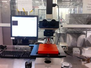
The Filmetrics F40-UV is a microscope-mounted thin-film measurement system, allowing you to non-destructively measure thin-film thicknesses in small (patterned) areas on your sample. It is an optical reflectometer, acquiring reflection spectra between 400-900nm optical wavelengths (Vis to Near-IR) with a regular halogen microscope light source. The Filmetrics software then performs curve-fitting to determine the thickness and/or refractive index of the measured films.
Capabilities
- Measure optically transparent thin-films down to ~30nm thickness.
- Microscope Objectives: 10x, 20x, 50x, 100x, 150x
- Acquire Optical Reflection Spectra from 400-900nm
- Spectrometer/Detector is capable of detecting down to UV ~190nm, but light source does not support this wavelength.
- Reflectivity curve-fitting for thin-film thickness analysis, supporting many common materials (Si3N4, SiO2 dielectrics, Si, GaAs, InP semiconductors, metals, photoresists etc.)
