Ashers (Technics PEII): Difference between revisions
→About: applicaitons section |
Added recipes, updated applications with times. |
||
| Line 10: | Line 10: | ||
}} |
}} |
||
= |
=About= |
||
These two parallel plate plasma etching systems are generally used to clean organic residue off of semiconductor wafers (ashing), etch organic films, or etch Si<sub>3</sub>N<sub>4</sub> films. The systems are both equipped with O<sub>2</sub> for organic removal / surface activation. |
These two parallel plate plasma etching systems are generally used to clean organic residue off of semiconductor wafers (ashing), etch organic films, or etch Si<sub>3</sub>N<sub>4</sub> films. The systems are both equipped with O<sub>2</sub> for organic removal / surface activation. |
||
| Line 16: | Line 16: | ||
One system also has CF<sub>4</sub>/O<sub>2</sub> 88% / 12% for etching Si<sub>3</sub>N<sub>4</sub>. These systems are operated manually and no sign-up is required. |
One system also has CF<sub>4</sub>/O<sub>2</sub> 88% / 12% for etching Si<sub>3</sub>N<sub>4</sub>. These systems are operated manually and no sign-up is required. |
||
=== |
===Mechanism=== |
||
This is |
This is a low-frequency RIE etch with O2 - using plasma ion bombardment, in a semi-vertical direction (although the higher 300mT pressure does attack sidewalls somewhat). The low kHz frequency allows ion to move with the RF, providing higher ion bombardment |
||
Low-temp (energy comes from ion acceleration, not temperature). |
Low-temp (energy comes from ion acceleration, not temperature). |
||
=== Applications === |
|||
Use this for situation where the material to be removed is resistant to chemicals (fluorocarbon polymers - think "plastic") and/or relatively hard (chlorinated PR, after a CL2/BCl2 etch), so physical bombardment is necessary to break up the material, or if high-temp is not acceptable. |
Use this for situation where the material to be removed is resistant to chemicals (fluorocarbon polymers - think "plastic") and/or relatively hard (chlorinated PR, after a CL2/BCl2 etch), so physical bombardment is necessary to break up the material, or if high-temp is not acceptable. Typical times: ~2min and microscope inspect and repeat. |
||
Stripping full-thickness PR's in the PEii is slow, at something like ~100nm/1min (at standard 100W/300mT). |
Stripping full-thickness PR's in the PEii is slow, at something like ~100nm/1min (at standard 100W/300mT). |
||
Surface activation, eg. making the surface hydrophilic before water-based wet-etching (15sec). This is very important for wet-etch processing through small, high aspect ratio photoresist holes or lines. |
Surface activation, eg. making the surface hydrophilic before water-based wet-etching (15sec), or dehydration of wafer surface before HMDS application. This is very important for wet-etch processing through small, high aspect ratio photoresist holes or lines. |
||
Increase adhesion of the next deposition (~2-4min), for example right before loading into evaporator for lift-off. Etch is a bit more aggressive and will go through any monolayers (organic or otherwise), and possibly slightly roughen the surface |
|||
| ⚫ | |||
| ⚫ | |||
| ⚫ | |||
| ⚫ | |||
| ⚫ | |||
| ⚫ | |||
== Recipes == |
|||
| ⚫ | |||
| ⚫ | |||
| ⚫ | |||
| ⚫ | |||
| ⚫ | |||
| ⚫ | |||
*Typical process conditions: |
*Typical process conditions: |
||
**Ashing: O2 300mT, 100W power, 30 sec. |
**Ashing: O2 300mT, 100W power, 30 sec up to 5 min. Make surface hydrophilic: same as above, 15-30sec |
||
**Si3N4 Etching: CF<sub>4</sub>/O<sub>2</sub> 300mT, 100W, ~ 100–150 nm / min. etch rate |
**Si3N4 Etching: CF<sub>4</sub>/O<sub>2</sub> 300mT, 100W, ~ 100–150 nm / min. etch rate |
||
Revision as of 02:05, 16 June 2022
| ||||||||||||||||||||||
About
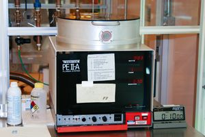
These two parallel plate plasma etching systems are generally used to clean organic residue off of semiconductor wafers (ashing), etch organic films, or etch Si3N4 films. The systems are both equipped with O2 for organic removal / surface activation.
One system also has CF4/O2 88% / 12% for etching Si3N4. These systems are operated manually and no sign-up is required.
Mechanism
This is a low-frequency RIE etch with O2 - using plasma ion bombardment, in a semi-vertical direction (although the higher 300mT pressure does attack sidewalls somewhat). The low kHz frequency allows ion to move with the RF, providing higher ion bombardment
Low-temp (energy comes from ion acceleration, not temperature).
Applications
Use this for situation where the material to be removed is resistant to chemicals (fluorocarbon polymers - think "plastic") and/or relatively hard (chlorinated PR, after a CL2/BCl2 etch), so physical bombardment is necessary to break up the material, or if high-temp is not acceptable. Typical times: ~2min and microscope inspect and repeat.
Stripping full-thickness PR's in the PEii is slow, at something like ~100nm/1min (at standard 100W/300mT).
Surface activation, eg. making the surface hydrophilic before water-based wet-etching (15sec), or dehydration of wafer surface before HMDS application. This is very important for wet-etch processing through small, high aspect ratio photoresist holes or lines.
Increase adhesion of the next deposition (~2-4min), for example right before loading into evaporator for lift-off. Etch is a bit more aggressive and will go through any monolayers (organic or otherwise), and possibly slightly roughen the surface
Detailed Specifications
- Gases used: CF4 / O2 (88%/12%) and O2
- ~ 10mT ultimate chamber pressure
- 100 kHz directly coupled excitation source
- Sample size: pieces to 6” wafers
- Gas flow and power control
Recipes
- Typical process conditions:
- Ashing: O2 300mT, 100W power, 30 sec up to 5 min. Make surface hydrophilic: same as above, 15-30sec
- Si3N4 Etching: CF4/O2 300mT, 100W, ~ 100–150 nm / min. etch rate
