**[//wiki.nanotech.ucsb.edu/w/images/3/34/DEMISJAN2020_-_Reticle_Layout_v1.GDS Here is an example GDS file (download)] for submission to the photomask manufacturer, with all objects moved to a single Layer.
**[//wiki.nanotech.ucsb.edu/w/images/3/34/DEMISJAN2020_-_Reticle_Layout_v1.GDS Here is an example GDS file (download)] for submission to the photomask manufacturer, with all objects moved to a single Layer.
*See the [[Stepper Mask-Making Guidelines (Generic)|Stepper Mask Making Guidelines page]] for an example of how to program this Reticle into an ASML Stepper job.
*See the [[Stepper Mask-Making Guidelines (Generic)|Stepper Mask Making Guidelines page]] for an example of how to program this Reticle into an ASML Stepper job.
==== Advanced Stepper Mask Layout ====
*[[Media:CAD Tutorial for ASML Reticle v2 DEMIS-DOE.OAS|CAD_Tutorial_for_ASML_Reticle_v2_DEMIS-DOE.OAS]] - example CAD file for reticle with many design variations.
**Cell "'''''Reticle_Layout'''''" shows the mask that would be printed by a photomask vendor. You would print '''Layers 1,2 and 3''' onto a single mask plate, with the CAD file origin at the center of the mask plate (no automatic centering).
**Cell "'''''Wafer_Layout'''''" shows an estimation/"simulation" of design variations to be exposed on the wafer. It is only a "simulation" because the real layout would be programmed on the Stepper tool itself, which may make changes (such as automatically filling to the wafer's edge).
*[[Media:ASML Reticle Programming Params - DEMIS-DOE v1.xlsx|ASML_Reticle_Programming_Params_-_DEMIS-DOE_v1.xlsx]] - stepper programming sheet for the above CAD file, for typing in the mask's '''''Images''''' into the Stepper software.
===CAD Files & Templates===
===CAD Files & Templates===
Revision as of 15:47, 29 April 2025
This page lists a few online calculators and utilities that are useful to lab users.
Boiling points of various compounds can tell you how volatile an etch product may be in a reactive ion etch, or whether they need to be wet-etched instead.
Enormous review of published wet etches of many semiconductors and alloys. The only thing it's missing is a hyperlinked table of contents.
Refractive Indices
Optical constants of many common materials. Useful for Optical thin-film analysis (ellipsometry/spectroscopic fitting), laser etch monitoring, optical filter/mirror/anti-reflection coating design, photonic devices etc.
A free, open-source, and fast/simple CAD tool for mask/reticle layout. Also has powerful functions, DRC, scriptiable and can handle very large files (GB's) efficiently.
Free editor for GDS, OASIS, DXF etc. available on Windows, MacOS, Linux.
Scriptable with Python, Ruby, C++
AutoCAD
Many photomask vendors can accept AutoCAD DWG files, but these can only be opened in AutoCAD (not KLayout or other layout programs). Although AutoCAD can produce a cross-compatible DXF file, we see many design/conversion issues with these files. This is because many shapes and line-types (Curves and Line/polyline/LWLine for example) used in AutoCAD don't convert as expected into the polygons needed for printing. Also the DXF file format itself often creates problems, such as incorrect scaling (undefined units: mm or µm?) or badly-filled/unclosed polygons.
CAD Design Tips
Cells and Instancing
All major chip layout programs support "Cells" and similar structures for hierarchical layout. It is highly recommended that you understand and use the concept of "Cells" in your design. This circumvents many problems with enormous file sizes (due to huge numbers of identical polygons), and if used properly, helps tremendously with programming the Stepper lithography machines. Links to documentation below:
OASIS files tend to be much smaller than GDS files, and they also save the Layer Names (not just number). Alternatively, in KLayout the function File > Save Session will save the entire view including layer styles and window/zoom locations will be saved. You can share this file, as the entire design file is embedded within it, but it may not be as robust between KLayout versions.
DXF Files can often cause problems because the format varies widely depending on the program they are exported from. For example, DXF can lose the "scaling" causing polygons to be 1000x larger than expected, or unexpectedly cause some shares to get filled in.
See the above page for important info on making "valid" CAD files, and setting up KLayout for efficient use.
Handling very large files
If you will be generating millions of identical shapes (eg. repeating array of circles), the file size can quickly become enormous due to all the stored polygon points. You can reduce the number of polygon points stored by:
Reduce the number of points in each shape/circle if possible.
Use Cell instancing so that only one, or a few, polygons are defined, and that same polygon is then only referenced as a repeating Cell instance. (See above for tutorials).
The OAS file type generates much smaller files, and most photomask vendors can accept this. Photomask vendors are used to handling large files.
Photomask vendors are able to take multiple files and insert them into the final reticle – you just need to provide a clear schematic showing the exact insertion coordinates for each file (with respect to the origin of each file). They can also do some boolean operations (for a fee).
Example CAD File
Here is an example CAD file, showing the use of Layers and Cells, designed in KLayout. The device is fictional, for illustrative purposes only.
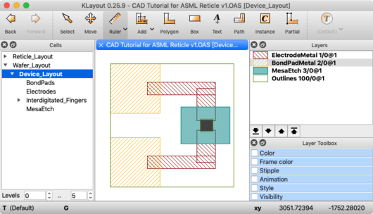
Cell "Device_Layout" shows a single device, with each Layer overlaid as it would be in a fabricated device. Each Layer (eg. a "process step" such as Mesa etch, Pad Metal etc.) is placed into it's own Cell.
"Device_Layout" Cell showing as the "top cell"
Every Cell's Origin (0,0) lies on top of one another in the final Device_Layout.
One way this can be accomplished is by selecting the objects/polygons you want to make into a new Cell, then use the function Edit >Selection > Make Cell, and uncheck the "Put Origin at..." checkbox, so the new Cell maintains the same origin as the original view.
The Cell "Reticle_Layout" can be exported by itself (right-click the Cell name), for sending to the photomask manufacturer.
Cell "Reticle_Layout" shows the mask that would be printed by a photomask vendor. You would print Layers 1,2 and 3 onto a single mask plate, with the CAD file origin at the center of the mask plate (no automatic centering).
Cell "Wafer_Layout" shows an estimation/"simulation" of design variations to be exposed on the wafer. It is only a "simulation" because the real layout would be programmed on the Stepper tool itself, which may make changes (such as automatically filling to the wafer's edge).
A free Matlab-like IDE and GUI, using the Python language. The Spyder interface is modeled after Matlab.
Includes the scientific Python libraries needed for array math (numpy), plotting (matplotlib), data science (pandas) and many others. Many open-source packages are available to extend capabilities. The PyVisa module adds equipment control capabilities for automated measurements.
A versatile online interpreter/calculator, allowing calculations such as "Volume of 1.5g of Silicon", "melting point of SiO2" or "520°C in Fahrenheit".
Python functions for returning n (refractive index) & k (extinction coefficient) of various NanoFab thin-films at a specified wavelength (aka. optical dispersion models)


