Filmetrics F40-UV Microscope-Mounted: Difference between revisions
→Screenshots + Examples: updated examples & confirming removal of SiO2 on Pt |
removed "screenshots" section --> "Examples" |
||
| Line 22: | Line 22: | ||
* [[Filmetrics F40-UV Quick Start|Quick Start Procedure]] |
* [[Filmetrics F40-UV Quick Start|Quick Start Procedure]] |
||
== |
== Examples == |
||
=== Good Curve-Fitting === |
=== Good Curve-Fitting === |
||
Revision as of 18:23, 31 May 2019
|
About
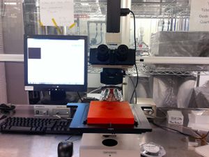
The Filmetrics F40-UV is a microscope-mounted thin-film measurement system, allowing you to non-destructively measure thin-film thicknesses in small (patterned) areas on your sample. It is an optical reflectometer, acquiring reflection spectra between 400-900nm optical wavelengths (Vis to Near-IR) with a regular halogen microscope light source. The Filmetrics software then performs curve-fitting to determine the thickness and/or refractive index of the measured films.
Capabilities
- Measure optically transparent thin-films down to ~30nm thickness.
- Microscope Objectives: 10x, 20x, 50x, 100x, 150x
- Acquire Optical Reflection Spectra from 400-900nm
- Spectrometer/Detector is capable of detecting down to UV ~190nm, but light source does not support this wavelength.
- Reflectivity curve-fitting for thin-film thickness analysis, supporting many common materials (Si3N4, SiO2 dielectrics, Si, GaAs, InP semiconductors, metals, photoresists etc.)
Operating Procedures
Examples
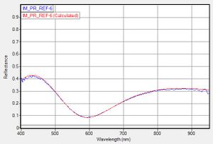
Good Curve-Fitting
Do not believe your thickness measurements unless the red/blue curves show a reasonably good match!


Checking whether a dry etch is complete
The F40-UV is very useful for measuring whether a thin-film has been completely removed during a dry etch. This is similar to using laser monitoring during the etch, except that the microscope enables you to measure inside small patterned areas that a laser monitor spot may not fit inside.
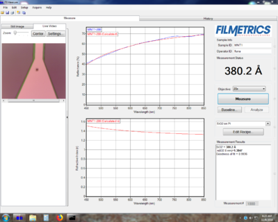
In the following example, we are trying to etch away the SiO2 from on top of a Platinum contact metal. The 20x objective allows us to measure the SiO2 thickness on top of the Platinum as we continue to etch in 1 minute increments, measuring in between etches.
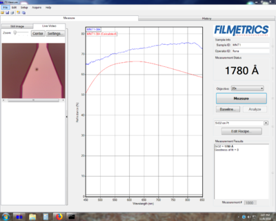
Finally, when the SiO2 has been fully removed, we see that we can't get a good fit between the measured (blue) and simulated (red) data.
Since the Platinum layer is thick enough to be opaque to visible light (>50nm), we just modelled this as SiO2 on top of Platinum, ignoring any other materials below the platinum.


