Contact Aligner (SUSS MA-6): Difference between revisions
Contact info changed to Lee S. |
verbiage and spec changes |
||
| Line 11: | Line 11: | ||
|toolid=33 |
|toolid=33 |
||
}} |
}} |
||
= |
==About== |
||
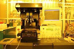
This system is a dual-use mask aligner and wafer-bond aligner. Mask alignment is used for contact and proximity exposure processes. Exposures can be |
This system is a dual-use mask aligner and wafer-bond aligner. Mask alignment is used for contact and proximity exposure processes. Exposures can be performed with gaps programmable from 10 um to 300 um in 1 um increments. Automatic wedge error compensation (WEC) is used to ensure that the mask and wafer are parallel. Lithography can be performed on wafers from 2” to 6” in diameter. Piece parts are better handled on the MJB-3 aligners. An automated image capture system is used for alignment at 5x, 10x, or 20x magnification. The system is fitted with visible, bottom-side optics for back-side alignment capability. The lamp is a 350 W Hg-Arc lamp, providing significant power in the g-h-and i-line regime. Integrated light level sensing ensures proper exposure doses as the lamp degrades. Bond alignment can be performed on 3” to 6” wafers. The bond alignment is performed with special fixturing to allow aligned samples to be transferred to the Karl-Suss SB6 system. |
||
| ⚫ | |||
| ⚫ | |||
*350 W Hg arc lamp, broadband exposure with Suss UV400 Optics |
*350 W Hg arc lamp, broadband exposure with Suss UV400 Optics |
||
*Automatic Light Intensity Drift Compensation |
*Automatic Light Intensity Drift Compensation: |
||
**Channel 1 is calibrated to 9 mW/cm² at 365 nm |
|||
*Programmable recipes |
|||
**Channel 2 is calibrated to 15 mW/cm² at 405 nm |
|||
*Programmable exposure gaps of |
*Programmable exposure gaps of 10-300 um in 1 um steps |
||
*Stored video imaging for precise, repeatable alignment |
*Stored video imaging for precise, repeatable alignment |
||
*Visible Back-Side Alignment System |
*Visible Back-Side Alignment System |
||
| Line 25: | Line 27: | ||
*Other wafer sizes can be discussed with staff |
*Other wafer sizes can be discussed with staff |
||
=Documentation= |
==Documentation== |
||
*[https://www.nanotech.ucsb.edu/wiki/Images/uploads/2018/Suss_MA6_SOP_Combined-1-4.pdf Suss MA-6 Standard Operating Procedure (SOP)] |
*[https://www.nanotech.ucsb.edu/wiki/Images/uploads/2018/Suss_MA6_SOP_Combined-1-4.pdf Suss MA-6 Standard Operating Procedure (SOP)] |
||
Revision as of 23:03, 11 September 2019
|
About
This system is a dual-use mask aligner and wafer-bond aligner. Mask alignment is used for contact and proximity exposure processes. Exposures can be performed with gaps programmable from 10 um to 300 um in 1 um increments. Automatic wedge error compensation (WEC) is used to ensure that the mask and wafer are parallel. Lithography can be performed on wafers from 2” to 6” in diameter. Piece parts are better handled on the MJB-3 aligners. An automated image capture system is used for alignment at 5x, 10x, or 20x magnification. The system is fitted with visible, bottom-side optics for back-side alignment capability. The lamp is a 350 W Hg-Arc lamp, providing significant power in the g-h-and i-line regime. Integrated light level sensing ensures proper exposure doses as the lamp degrades. Bond alignment can be performed on 3” to 6” wafers. The bond alignment is performed with special fixturing to allow aligned samples to be transferred to the Karl-Suss SB6 system.
Detailed Specifications
- 350 W Hg arc lamp, broadband exposure with Suss UV400 Optics
- Automatic Light Intensity Drift Compensation:
- Channel 1 is calibrated to 9 mW/cm² at 365 nm
- Channel 2 is calibrated to 15 mW/cm² at 405 nm
- Programmable exposure gaps of 10-300 um in 1 um steps
- Stored video imaging for precise, repeatable alignment
- Visible Back-Side Alignment System
- Lithography for 2” to 6” diameter wafers
- Bond alignment for 3” to 6” wafers, integrates with SB6 bond
- Other wafer sizes can be discussed with staff
