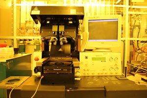
Contact Aligner (SUSS MA-6)
| ||||||||||||||||||||||||||||||
| |
| |
|
| |
| |
|
About
This system is a dual-use mask aligner and wafer-bond aligner, used for contact and proximity exposure processes. System is motorized for contact/proximity, microscope objective movement and exposure, with a computer used to display the microscope image for regular and backside alignment overlay. Exposures can be performed with gaps programmable from 10 um to 300 um in 1 um increments. Automatic wedge error compensation (WEC) is used to ensure that the mask and wafer are parallel. The lamp is a 350 W Hg-Arc lamp, providing significant power in the g-h-and i-line regime. Integrated light level sensing ensures proper exposure doses as the lamp degrades.
Lithography can be performed on wafers from 2” to 6” in diameter. Piece parts are better handled on the MJB-3 aligners.
The system is fitted with visible, motorize, bottom-side optics for back-side alignment capability. Backside alignment is performed with an automated image capture system, at 5x, 10x, or 20x magnification. The backside alignment system takes images of the photomask from the underside, then overlays that image digitally with the wafer face-down, again aligning with the cameras on the underside.
Bonding alignment can be performed on 3” to 6” wafers. The bond alignment is performed with special fixturing to allow aligned samples to be transferred to the Karl-Suss SB6 system - contact the supervisor beforehand so the bond alignment fixturing can be installed.
Detailed Specifications
- 350 W Hg arc lamp, broadband exposure with Suss UV400 Optics (350 - 450 nm)
- Resolution (per Manufacturer*):
- * Resolution achieved on 150 mm Si-wafer with 1.2 µm thick AZ 4110
- Vacuum Contact: <0.8 µm
- Hard Contact: <1.5 µm
- Soft Contact: <2.5 µm
- Proximity (@ 20 µm): <3.0µm
- Topside alignment accuracy: down to 0.5 µm
- Backside alignment accuracy: down to 1 µm
- Stage mechanical accuracy: 0.1 μm (step size)
- Automatic Light Intensity Drift Compensation:
- Channel 1 is calibrated to 9 mW/cm² at 365 nm
- Channel 2 is calibrated to 15 mW/cm² at 405 nm
- Programmable proximity exposure gap of 10-300 µm in 1 µm steps
- Programmable alignment gap of 1 - 999 µm in 1 µm steps
- Stored video imaging for overlay alignment
- Visible Back-Side Alignment System
- Lithography for 1” to 6” diameter wafers - 6 mm maximum thickness
- Pieces down to 5 x 5 mm - Please be aware of the stage movement range: X ± 10mm, Y ± 5 mm
- TSA objective separation: 32 - 160 mm
- BSA objective separation: 15 - 100 mm
- Chuck Sizes:
- 1" square (or wafer) and smaller, backside alignment capability
- 3" wafer, no backside alignment
- 4" wafer, backside alignment capability
- 6" wafer, backside alignment capability
- Mask Holder Sizes:
- 3"
- 4"
- 5" mask - can be modified to support a 6" mask but exposure area will still be ~4" diameter (see Staff)
- 7"
- Bond alignment for 4” to 6” wafers, integrates with SB6 bonder
- Other wafer sizes can be discussed with staff
Operating Procedures
- MA6 Standard Operating Procedure, includes Back-Side Alignment
- MA6 Exposure Mode Information
- MA6 Backside Alignment - Allowed Mark Locations
- BA6 Standard Operating Procedure
Mask Plate Info
- Mask Making Guidelines - Contact Masks - in progress
- Photomask Ordering Procedure for UCSB Users - see this page for how to submit your order into the UCSB purchasing system.
CAD Files
For designing your mask plates.
- Male/female alignment marks (GDS): MA6-FrontBack_AlignMarks_only.gds
- CAD Layout Programs
- CAD Design Tips
- CAD Files & Templates - alignment markers, verniers and other useful CAD objects
Recipes
- Recipes > Lithography > Suss MA6
- Also lists the exposure powers.
- Photolithography - Manual Edge-Bead Removal Techniques
