Make your CAD file of your device according to the tool you're going to do litho on.
Make separate "Layers" on your CAD file corresponding to each litho.
Fill out the Mask Order Form for the photomask vendor you choose to order from. Can order all photomasks (one for each Layer) in one order, calling out separate CAD Layers for each Mask.
Academic users: Contact Demis for quotes from photomask vendors.
Industrial users: Contact photomask vendors for quotes, we can suggest some or you can find them online yourself.
UCSB Users: Submit a requisition in Procurement Gateway to send a PO to the photomask vendor.
Send Photomask vendor your CAD file and Mask order form (referencing above PO).
Industrial Users: You can pay by credit card if desired.
Typically ~3 days to receive the photomasks.
Generic Contact Mask Parameters
For the contact aligner you are designing for, make sure you know the following specifications:
Mask Plate Size
We have two different styles of contact aligners and each has it's own capability in regard to the substrate and mask size it can accommodate (with some overlap between the two).
SUSS MJB-3:
Wafer size: 3" max. for vacuum mode; 4” for soft contact (3” x 3” exposure area)
Substrate size: 3" x 3" max
Mask plate size: 3" x 3" x 0.090" or 4" x 4" x 0.090", typically soda-lime glass.
SUSS MA-6:
Chuck Sizes:
1" square (or wafer) and smaller, backside alignment capability
3" wafer, no backside alignment
4" wafer, backside alignment capability
6" wafer, backside alignment capability
Mask Holder Sizes:
3"
4"
5" mask - can be modified to support a 6" mask but exposure area will still be ~4" diameter (see Staff)
7"
The plate size should be ~1" larger than your wafer size, AND the contact aligner should have a plate holder compatible with that plate size. Some examples:
To expose a 2" (50mm) wafer, or smaller pieces you could order
A 3 " or 4" mask plate. Eg. 3 x 3 x 0.090 inch soda limeglass.
Either put your design in the center of the plate, and order multiple plates (one for each process step/"Layer"), or
Put multiple patterns on a single plate and use the offset-vacuum chuck, to put your sample under the right pattern on the plate. (This takes a bit more experience with the MJB to design correctly.)
To expose a 3" (75mm) wafer, you could order
A 4" or 5" mask plate. Eg. 5 x 5 x 0.090 inch soda limeglass.
To expose a 4" (100mm) wafer, you should order
5" mask plate. Eg. 5 x 5 x 0.090 inch soda limeglass.
Either the quoted product number from our photomask vendor quotes, or the minimum feature size in your CAD - and just ask the photomask vendor which product number to use.
Other Mask Plate Specs
For all contact plates, we suggest the following standard params:
Material: Soda Lime glass (quartz is generally overkill)
Thickness 0.090" (eg. 5" x 5" x 0.090" or 4" x 4" x 0.090")
Orientation/Mirroring should be "Right Reading with Chrome Down" if your CAD file shows exactly what you want on your wafer.
For Back side alignment, don't forget to mirror your pattern horizontally/over the Y-axis (since your wafer will be flipped).
You can choose whether the polygons you draw are transparent glass ("objects are clear") or opaque chrome ("objects are dark"). You must consider whether you are using a positive or negative resist.
Ask the tool's Process Expert or Tool Supervisor to confirm these values. You can send your draft order form and CAD file to the tool super/process expert for review.
Definitions for Mask/Reticle Order Form
When submitting the photo mask order, the following notes & definitions apply:
"Grade" or "Product Code" will be one of the items on our quote. This will specify the glass type (soda-lime or quartz), plate size (4" square and 0.090" thick, for example), and the resolution. The grade choice determines the price, and is chosen based on required feature size (smaller feature size is more expensive). This is found on the vendor's quote, or you ask the vendor for a price based on desired minimum feature size (smallest feature actually present on your CAD file).
Although you will submit your CAD file at 1x wafer scale, the actual reticle is printer larger by the stepper's magnification (eg. 4x or 5x mag, depending on the stepper system), so make sure to choose your reticle grade accounting for this; eg. If my CAD has 1.0µm lines smallest feature, I should choose a photomask grade better/equal to 4.0µm for a stepper with 4x reduction.
"Title" or "Device Name" or "Layer Title" - any text of your choosing, to identify this "set" of multiple mask plates ("Device Name") and each individual mask plate of the set ("Layer title").
Eg. "Device" is "DFB Laser 2025-01"
"Layer Titles" may be "Mesa etch", "Contact pads" and "Gratings" etc.
The mask plates will show both, eg. one plate will show "DFB Laser 2025-01: Mesa Etch" and another will have ""DFB Laser 2025-01: Gratings", printed on the edge of the plates.
“GDS Level” is also known as “layer number” - the GDS Layer number to print, from your CAD file
If you are printing multiple mask plates for separate device Layers, you can submit one CAD file with each Layer on a separate GDS Layer, and specify each GDS Layer number as a separate plate (with it's own Title text, polarity, grade/CD etc.) on the Order form (on it's own line).
"topcell" or "structure name" is the Cell in your CAD file that contains the hierarchy of patterns to print.
Polarity/Mirroring should be "Right-Reading (legible text) with Chrome Down", if your CAD is exactly what you want on the wafer, for all our systems.
“Min. Feature on Mask” refers to minimum clear or opaque feature, assuming features similar to lines/spaces. This should be specified at the reticle-scale - see "Grade" above.
“Min. Contact” refers to features with aspect ratio close to 1:1, eg. Squares and circles. These have a separate spec due to the manufacturing process, so make sure to choose the appropriate grade of photomask with this in mind.
“CD”, or "Critical Dimension" - Choose a CD similar to your most critical feature (scaled to the reticle scale), so the vendor will print & measure & guarantee test structures at that exact size.
Academic users may request the UCSB Nanofab's quotes from various photomask vendors.
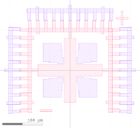
On-wafer alignment marks: You will need matching male+female alignment marks to match each mask plate to on-wafer layers. You can use any alignment mark design you want - some examples are linked below.
CAD Files
For designing your mask plates.
CAD Files & Templates - alignment markers, alignment verniers and other useful CAD objects
By default, Wafer flat is Down (–Y) with respect to your CAD file for most systems.
Utilize the "Cell" and "Cell Instancing" functionality in your CAD layout program! (aka. a "Block" in AutoCAD). Highly recommended to use KLayout, not AutoCAD. See Calculators + Utilities > CAD Design Tips for tutorials.
Center your entire design around the coordinates (0,0). (0,0) should always be the center of your device, wafer and/or photomask/reticle Cells. Photomask vendors can then NOT "auto center" your designs on the plate.
Inside each sub-Cell, also design around the cell's (0,0) origin.
Create a Cell called "reticle_layout" or similar, that is an exact representation of what the printed reticle patterns should look like (typically at 1x wafer-scale, if not including the outer templates for the stepper system). Instance the Device's Cells into reticle_layout, and reference this Cell on your mask order form. (You can also Instance the same cells into "device_layout" and "wafer_layout" cells during design/verification.).
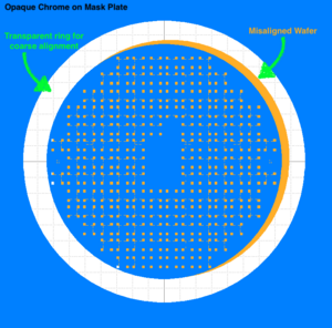
First Layer Alignment
To align your first layer, when there are no alignment marks on your wafer, it is very helpful to leave CLEAR/transparent open areas around the wafer to allow you to see the outer edges of your wafer/sample for coarse alignment to the pattern. Example below:Example of transparent ring on mask plate for first layer alignment.However, make sure to consider the process implications for the fact that photoresist on this outer ring will be exposed during exposure (ie. may get developed out or hardened, depending on positive/negative photoresist).