Photolithography - Manual Edge-Bead Removal Techniques
Purpose of Edge Bead Removal
Removing the thicker photoresist along the edges of your sample (aka. edge-bead removal, EBR) has multiple advantages:
- These techniques are required for loading full-wafers into etchers that use top-side clamps, to prevent photoresist from sticking to the clamp (and potentially destroying your wafer).
- For contact lithography, this improves the proximity of the mask plate and sample, improving resolution.
- For some projection systems, such as the Maskless Aligner, EBR can help with autofocus issues.
Razor Blade
Use a razor blade to scrape off the edge-bead regions. This works well for small samples, if the substrate material is not fragile (works well for Silicon, Sapphire, GaAs, Silica etc.).
Especially useful for photoresists that don't chemically dissolve easily, such as PMGI, SU8, BCB.
EBR100 Swabbing
AZ EBR100 squirt bottles can be found on the spinner benches. (Do NOT bring Acetone onto the spin-benches! The fumes affect nearby PR.) Only use this chemical in a fume hood, and dispose in the waste in the fume hood waste containers.
EBR100 dries quickly without wicking onto the wafer/PR, so is preferred for edge-bead removal.
- Squirt some EBR onto a COTTON swab (not plastic swab! They will dissolve.)
- Roll the swab on a cleanwipe to remove excess liquid.
- Use the swab like a paintbrush to remove PR from the edge of the wafer, re-soaking as needed.
- Better to remove TOO MUCH edge-bead than too little - high chance of wafer sticking to machine clamp if you remove too little.
Lithographic Edge Bead Removal
This method significantly lowers the risk of breaking a wafer in clamped systems such as the DSEiii or Fluorine Etcher.
This process only removes the outermost photoresist for Positive PR's. For Negative PR's, your should design you litho so there is no exposure on the outer 7mm, so the PR is automatically removed during develop.
For small parts (1-2 cm) square or irregularly shaped, you can cut pieces of tinfoil into small squares, and mask all but 2 edges and flood expose those two edges (on a contact aligner), then repeat for the other two edges. Expose with 3-5x the typical dose, since the PR is thick at the edge. Then develop the sample to remove the edge bead. Subsequent litho will work fine.
For larger parts (eg. full wafers), you will want to make a custom plastic or metal mask that you can place on top of the wafer during flood expose - then develop to remove the edge-bead.
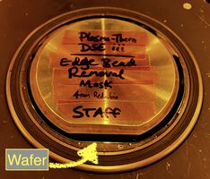
We do have simple metal masks made for 4-inch wafers, that you can use on the Suss MA6 for I-Line Flood Expose mode or on the DUV Flood Expose to expose your edge bead. The metal mask is stored in Bay7, in the bottom-most blue Vidmar drawers between the Suss MA6 & GCA Stepper #1, in a transparent cassette labeled “edge bead removal mask”. We require the "4mm recessed" mask for clamp systems.
| Location of our edge-bead removal mask | |
|---|---|

|

|
| Using the mask on the MA-6 with Flood Exposure mode. | |

|

|
I-Line Photo-EBR Process
- Spin/cure an I-Line photoresist using your standard photolith. params (for example SPR 220-3).
- Don't load a mask plate.
- Turn off "Load Mask" mode - you will likely need to confirm that no mask is present.
- Place the wafer on the MA-6 Contact Aligner with the metal mask in place.
- You will use [Lamp Test] for the exposure. You can also use "Flood Expose" program and type in an exposure time.
- Expose for about 3-2x longer than your normal exposure time.
- Load wafer into your I-Line exposure tool & Expose your process
- Run your PEB and Develop as per your normal process.
- (If you did not develop the EBR yet, it should go away in this step.)
DUV Photo-EBR Process
- Spin/cure a DUV photoresist using your standard photolith. params (for example UV6).
- Place the wafer on the DUV Flood Exposer with the metal mask in place.
- Turn on rotation on slow (so mask doesn't move), lamp warmup is not required.
- Expose for 13 sec, with slow rotation.
- Optionally: PEB 135°C, 60sec, Develop, dry (in SRD), then proceed. This did not affect my primary lithography when I did this step separately. I've also done photo-EBR where I combined this EBR exposure with the primary Imaging litho. and only did a single develop.
- Load wafer into ASML & Expose your process
- PEB 135°C, 90sec
- 300MiF develop as per your normal process.
- (If you did not develop the EBR yet, it should go away in this step.)
Small-Sample (<1cm) PR spinning
For very small samples, the edge-bead can take up almost all of the sample surface! Here is a technique used by many lab users to mitigate this.
Preparation:
- Prepare some "shim" pieces of the same thickness (within ~50µm) as your sample.
- Use the drop-gauge in Bay 6 or Bay 4 to measure thickness.
- Either make 4 long pieces, or 8 identical pieces as your sample.
- This may require dicing some dummy material.
Spinning:
- Cut a 2 in. Square piece of low tack blue tape (aka. "dicing tape"), you find this on dispensers between the ovens in Bay 6.
- Place the blue tape Sticky side up on the bench, usually photo resist bench.
- Mount your sample in the center. (make sure back of sample is clean.)
- Mount Shim samples (prepared above) around it on all sides.
- Minimize gap between sample and shims.
- Mount the entire assembly onto spinner vacuum chuck and spin PR.
- Do a test spin without PR first to make sure pieces are held well.
- Use vacuum chuck with large enough vacuum to cover ~1 inch area.
- Remove sample from assembly to bake the photoresist.
Demis D. John, 2018-10-22; Updated 2025-12-05.