DSEIII (PlasmaTherm/Deep Silicon Etcher): Difference between revisions
→Recipes: fixed recipes link |
Text replacement - "www.nanotech.ucsb.edu/wiki/" to "wiki.nanotech.ucsb.edu/wiki/" |
||
| Line 34: | Line 34: | ||
= Recipes = |
= Recipes = |
||
* [https:// |
* [https://wiki.nanotech.ucsb.edu/wiki/index.php/ICP_Etching_Recipes#DSEIII_.28PlasmaTherm.2FDeep_Silicon_Etcher.29 Plasma-Therm DSE-iii Recipes] - Recipes specific to this tool. |
||
* All [[Dry Etching Recipes]] - use this list to see other options for dry etching various materials. |
* All [[Dry Etching Recipes]] - use this list to see other options for dry etching various materials. |
||
Revision as of 01:29, 7 April 2020
| |||||||||||||||||||||
About
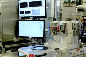
The Si DRIE system is a Plasma-Therm DSEIII series system with a loadlock. The system has an Inductively Coupled Plasma (ICP) coil and a capactively coupled substrate HF (13.56MHz) and LF (100kHz) supplies to independently control plasma density and ion energy in the system. This system is dedicated to....... The fixturing is configured for 4" diameter Si wafers and uses a clamp to hold the sample on the RF chuck.
The materials allowed in the system are limited to Silicon, SiO2, Si3N4, SiOXNY, and polymer films such as photoresist, PMMA, and polyimide. Other materials can be placed in the chamber.........
Helium back-side cooling is used to keep the sample cool during the etch. Temperature control is very important as the polymer passivation layer is chemically etched away by the fluorine gas at elevated temperatures, resulting in loss of profile control. Pieces of wafers can be mounted onto 4" silicon wafers using .......... The etch rate is dependent on the open area of silicon (macro-loading effect) with large open area samples etching slower than small open area samples. Features with a high aspect ratio will also etch slower than more open areas. This is known as RIE lag or the micro-loading effect.
Detailed Specifications
- 3500 W ICP coil power at 2 MHz and 500 W substrate bias at 13.56 MHz plasma generators
- C4F8, SF6, O2, Ar, N2 gases available
- He-back-side cooling
- Windows-based Cortex software control of process and wafer handling
- Allowed materials: Silicon, SiO2, Si3N4, SiOXNY, and polymer films such as photoresist, PMMA, and polyimide; ..........
- Realized etch rates (including passivation steps) for Bosch process of >8 um / min. Selectivity to resist > 80:1 for low aspect ratio.
- Laser monitoring with camera and etch simulation software for SOI etching - Intellemetrics
Documentation
Recipes
- Plasma-Therm DSE-iii Recipes - Recipes specific to this tool.
- All Dry Etching Recipes - use this list to see other options for dry etching various materials.
