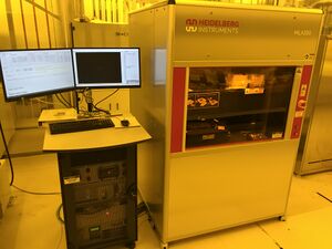
Maskless Aligner (Heidelberg MLA150): Difference between revisions
Added photo |
→About: minor updates |
||
| Line 11: | Line 11: | ||
}} |
}} |
||
==About== |
==About== |
||
The MLA150 allows for arbitrary direct patterning of I-Line photoresists, directly from |
The MLA150 allows for arbitrary direct patterning of I-Line photoresists, directly from an uploaded CAD drawing/file (GDS, DXF, CIF etc.). The system uses a [https://en.wikipedia.org/wiki/Digital_micromirror_device digital micromirror device] ("DMD", an array of MEMS mirrors) for patterning the exposure light-field, to programmatically expose digitized patterns directly onto the sample - no glass photomasks/reticles are required. |
||
The system has a continuous, automatic autofocus, using either a pneumatic or optical detection. This enables lithography on non-planar or curved substrates. We also have the high-aspect ratio (variable/long focal length) option installed for very thick (~70µm) photoresists. |
The system has a continuous, automatic autofocus, using either a pneumatic or optical detection. This enables lithography on non-planar or curved substrates. We also have the high-aspect ratio (variable/long focal length) option installed for very thick (~70µm) photoresists. |
||
Depending on the exposure options and write area, MLA is able to expose a 100mm wafer in about 30min, and achieves minimum features sizes around 0.5µm, with overlay/alignment accuracy better than 200nm. |
Depending on the exposure options and write area, the MLA is able to expose a 100mm wafer in about 30min, and achieves minimum features sizes around 0.5µm, with overlay/alignment accuracy better than 200nm. Arbitrary drawings can be exposed onto any feature located on the microscope. |
||
Lastly, the greyscale lithography is possible, producing repeatable, slanted or tapered structures in photoresist or photo-active dielectrics like SU-8. |
Lastly, the greyscale lithography is possible, producing repeatable, slanted or tapered structures in photoresist or photo-active dielectrics like SU-8. |
||
| Line 24: | Line 24: | ||
*Wafer / substrate thickness: |
*Wafer / substrate thickness: |
||
*Exposure optics: |
*Exposure optics: |
||
**[https://en.wikipedia.org/wiki/Digital_micromirror_device Digital micromirror device (DMD)] |
|||
**Laser #1: 375nm |
**Laser #1: 375nm |
||
**Laser #2: 405nm |
**Laser #2: 405nm |
||
* Focus modes: |
* Focus modes: |
||
** Extended Focus Range |
|||
* Alignment: |
|||
** Variable Focal Depth |
|||
** Modes? |
|||
* Alignment Accuracy: ≤ 200nm |
|||
** Repetability |
|||
*Additional manufacturer options: |
*Additional manufacturer options: |
||
** |
**High-resolution option |
||
**Dual lasers? |
|||
**High-resolution option? |
|||
* Uniformity: |
|||
* Write speeds: |
|||
==Documentation== |
==Documentation== |
||
*[[MLA150 - Standard Operating Procedure]] |
*[[MLA150 - Standard Operating Procedure]] |
||
Revision as of 05:49, 3 October 2020
 Work In Progress This article is still under construction. It may contain factual errors. Content is subject to change. |
|
About
The MLA150 allows for arbitrary direct patterning of I-Line photoresists, directly from an uploaded CAD drawing/file (GDS, DXF, CIF etc.). The system uses a digital micromirror device ("DMD", an array of MEMS mirrors) for patterning the exposure light-field, to programmatically expose digitized patterns directly onto the sample - no glass photomasks/reticles are required.
The system has a continuous, automatic autofocus, using either a pneumatic or optical detection. This enables lithography on non-planar or curved substrates. We also have the high-aspect ratio (variable/long focal length) option installed for very thick (~70µm) photoresists.
Depending on the exposure options and write area, the MLA is able to expose a 100mm wafer in about 30min, and achieves minimum features sizes around 0.5µm, with overlay/alignment accuracy better than 200nm. Arbitrary drawings can be exposed onto any feature located on the microscope.
Lastly, the greyscale lithography is possible, producing repeatable, slanted or tapered structures in photoresist or photo-active dielectrics like SU-8.
Detailed Specifications
- Wafer size:
- Wafer / substrate thickness:
- Exposure optics:
- Digital micromirror device (DMD)
- Laser #1: 375nm
- Laser #2: 405nm
- Focus modes:
- Extended Focus Range
- Variable Focal Depth
- Alignment Accuracy: ≤ 200nm
- Additional manufacturer options:
- High-resolution option
Documentation
Design Tools/Info
Recipes
- Recipes > Lithography > Maskless Aligner MLA150
- Starting recipes for various I-Line photoresists
