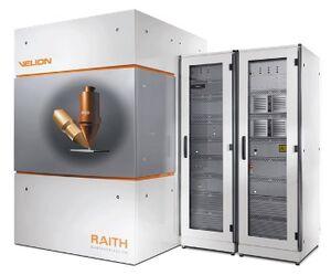
Focused Ion-Beam Lithography (Raith Velion): Difference between revisions
Jump to navigation
Jump to search
Content deleted Content added
No edit summary |
|||
| Line 13: | Line 13: | ||
= About = |
= About = |
||
The Raith Velion ion beam tool was installed at UCSB in 2020 and signed off and avaiable for. use in early 2021. |
The Raith Velion ion beam tool was installed at UCSB in 2020 and signed off and avaiable for. use in early 2021. |
||
This system uses the vector scan approach for electron beam deflection within a field, step and repeat for stage movement between fields, the combination of which allows the entire area of the sample to be exposed to the electron beam. |
|||
The machine can be run at 25, 50 and 100 kV. Note however that only the 100kV mode is used at UCSB. |
|||
=Detailed Specifications= |
=Detailed Specifications= |
||
Revision as of 14:49, 12 March 2021
 Work In Progress This article is still under construction. It may contain factual errors. Content is subject to change. |
|
About
The Raith Velion ion beam tool was installed at UCSB in 2020 and signed off and avaiable for. use in early 2021.
Detailed Specifications
nanoFIB column:
- Liquid Metal Alloy Ion Sources (LMAIS) providing ions for Gallium-free patterning (Au, Si)
- High resolution patterning capabilities (minimum feature size < 15nm)
- Fully corrected write fields (distortion, stigmation)
- Long term current stability (days)
Laser Interferometer stage:
- Mechanical movement at 1nm precision
- Continuous stage modes for stitch free FIB patterning on full 4”wafer scale
- Stitching and overlay accuracy: < 50 nm ( mean+3 sigma)
FE SEM
- Process control for rapid prototyping
Additional Capabilities:
- Automated height sensing to detect sample surface height variation for automated correction
- Pt Gas Iinjection System (GIS) deposition
- Raith Nanosuite software incl. CAD (GDSII) navigation & patterning
Recipes
- Recipes > Lithography > FIB Lithography
- Contains starting recipes etc.
