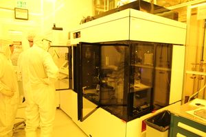
Stepper 2 (AutoStep 200): Difference between revisions
Abrahamsen (talk | contribs) No edit summary |
Abrahamsen (talk | contribs) No edit summary |
||
| Line 31: | Line 31: | ||
*[http://signupmonkey.ece.ucsb.edu/wiki/index.php/Lithography_Recipes Process Page] |
*[http://signupmonkey.ece.ucsb.edu/wiki/index.php/Lithography_Recipes Process Page] |
||
=Service Provider= |
|||
=See Also= |
|||
* [http://3ctechnical.com/index.html 3C Technical] - The company that services the stepper. |
* [http://3ctechnical.com/index.html 3C Technical] - The company that services the stepper. |
||
Revision as of 17:46, 1 April 2014
|
About
Our GCA wafer stepper is an i-line (365 nm) step and repeat exposure tool for doing lithography that requires high resolution and/or critical alignment. The system has been modified to accept piece parts (down to ~15 mm x 15 mm) up to 6” diameter wafers using manual wafer loading. The maximum die size is ~ 15 mm x 15 mm. The system has an Olympus 2142 (N.A. = 0.42) lens that reduces the mask image by 5 x and gives an ultimate resolution of ~ 0.5 um in the center of the lens field. The system can easily produce 0.7 um isolated lines across the entire field. Autofocus is used to determine the sample surface relative to the lens, making the focus stable and repeatable for different thickness of wafer. The stages are controlled by stepper motors and laser interferometers. Using the global, manual alignment, better than 0.25 um alignment error is achievable. Using the DFAS local alignment system, alignment error better than 0.15 um is achieved. With the 350 W Hg arc lamp, we get about 180 W/cm² of i-line intensity at the wafer.
The system is computer controlled with the capability to program and save a wide variety of exposure jobs. We also have unlimited phone support for system problems through a service contract. The laboratory contains a variety of i-line compatible photoresists. SPR510A, 955CM, 950-0.8 for 0.7-1.0 um thick positive processes. AZ5214E for 1.0 um thick image reversal (negative) process. SPR955CM-1.8 for 1.5-2.0 um thick positive processes. SPR220-3 for 2.5-5 um thick positive process. SPR220-7 and AZ9260 for >5 um thick positive processes. AZnLOF5510 for <1.0um and AZnLOF 2020 for 1.5-3 um negative resist process. Shipley LOL-2000 is also used as an underlayer for high resolution lift-off processes.
Detailed Specifications
- Lens: Olympus 2145: NA = 0.45; Depth of field = 1.2 um for 0.6 um process
- Maximum die size: ~ 15 mm x 15 mm
- Resolution: 400-450 nm for R&D; 700 nm over entire 15 mm x 15 mm field
- Registration tolerance: 0.30 mm global alignment; Max 0.15 mm local alignment (with care, you can achieve < 0.10 mm registration)
- Minimum substrate size: ~ 10 x 10 mm
- Computer programmable, recipes saved on hard disk
- Reticle alignment fiducials and global/local fiducials available
Process Information
Service Provider
- 3C Technical - The company that services the stepper.
