Molecular Vapor Deposition: Difference between revisions
Jump to navigation
Jump to search
Content deleted Content added
Created page with "{{tool|{{PAGENAME}} |picture=MVD.jpg |type = Vacuum Deposition |super= Aidan Hopkins |phone=(805)839-3918x208 |location=Bay 4 |email=hopkins@ece.ucsb.edu |description = Molecular…" |
No edit summary |
||
| Line 7: | Line 7: | ||
|email=hopkins@ece.ucsb.edu |
|email=hopkins@ece.ucsb.edu |
||
|description = Molecular Vapor Deposition System |
|description = Molecular Vapor Deposition System |
||
|manufacturer = |
|manufacturer = [http://www.appliedmst.com/ Applied Microstructures Inc.] |
||
|materials = |
|||
|materials = [http://www.appliedmst.com/ Applied Microstructures Inc.] |
|||
}} |
}} |
||
= About = |
= About = |
||
Revision as of 15:20, 10 July 2012
| ||||||||||||||||||||
About
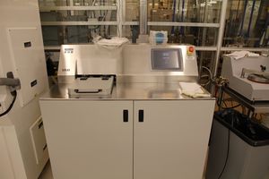
The Molecular Vapor deposition system is used for deposition of a monolayer-thick fluorocarbon film for producing extremely hydrophobic surfaces used for anti-sticking layers for nanoimprinting or anti-stiction layers for MEMS. The system has integrated Oxygen plasma cleaning for organic removal and surface activation and can be run at temperatures up to 80°C. Multi-step recipes can be created. The system is currently configured for FDTS (perflourodecyltricholorsilane) and water to producing the coatings. Up to 6” wafers can be coated in the system.
