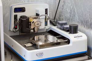
Atomic Force Microscope (Bruker ICON)
| ||||||||||||||||||||||||||||||
About
The Bruker ICON AFM utilizes the latest paradigm in Atomic Force Microscopy - PeakForce Tapping®, a method that combines the best features of the legacy Contact Mode and Tapping Mode imaging techniques, namely direct force control and intermittent surface contact to reduce damaging lateral forces, to precisely control the probe-to-surface force interaction as pixel-to-pixel force curve measurements. This control results in the most consistent, highest resolution AFM imaging technique that can be used on a wide range of sample types.
Note that the ICON AFM also can also utilize the legacy ContactMode and TappingMode techniques for imaging if required.
In PeakForce Tapping®, the probe periodically taps the sample and the pN-level interaction force is measured directly by the deflection of the cantilever. Through superior force control, the feedback loop keeps the peak force constant, down to pN range, in both air and fluid, which is significantly lower than is typically used with other modes, such as TappingMode™, in the 1-10 nN range. PeakForce Tapping® enables the researcher to precisely control probe-to-sample interaction, providing the lowest available imaging forces.
Detailed Specifications
- PeakForce Tapping® imaging for superior resolution and consistency
- Legacy Contact Mode and Tapping Mode imaging also available
- Substrate size range: small pieces (>2mm) up to 4" wafers
- Computer controlled XY stage for superior sample positioning; piezo Z scan range ~ 12um
- Basic electrical measurement techniques are available but only using Contact Mode imaging.
- Scanning Capacitance Microscopy (SCM)
- Conductive AFM (CAFM) for high currents, Tunneling AFM (TUNA) for low currents
