Filmetrics F40-UV Microscope-Mounted

From UCSB Nanofab Wiki
Revision as of 04:39, 24 May 2019 by John d (talk | contribs) (→‎Screenshots + Examples: Added example of inspecting for SiO2 dry-etch completion.)
Jump to navigation Jump to search
Filmetrics F40-UV Microscope-Mounted
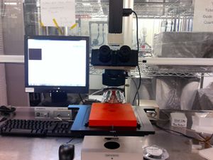
Filmetrics F40-UV - system pic 01.jpg
Tool Type Inspection,_Test_and_Characterization
Location Bay #4
Supervisor Ning Cao
Supervisor Phone (805) 893-4689
Supervisor E-Mail ningcao@ece.ucsb.edu
Description Measures surface topography, step heights and roughness with white-light interferometry.
Manufacturer Filmetrics Inc.
Model F40-UV


About

The Filmetrics F40-UV is a microscope-mounted thin-film measurement system, allowing you to non-destructively measure thin-film thicknesses in small (patterned) areas on your sample. It is an optical reflectometer, acquiring reflection spectra between 400-900nm optical wavelengths (Vis to Near-IR) with a regular halogen microscope light source. The Filmetrics software then performs curve-fitting to determine the thickness and/or refractive index of the measured films.

Capabilities

  • Measure optically transparent thin-films down to ~30nm thickness.
  • Microscope Objectives: 10x, 20x, 50x, 100x, 150x
  • Acquire Optical Reflection Spectra from 400-900nm
  • Spectrometer/Detector is capable of detecting down to UV ~190nm, but light source does not support this wavelength.
  • Reflectivity curve-fitting for thin-film thickness analysis, supporting many common materials (Si3N4, SiO2 dielectrics, Si, GaAs, InP semiconductors, metals, photoresists etc.)

Operating Procedures

Screenshots + Examples

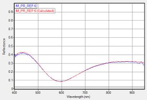
example spectrum curve fit
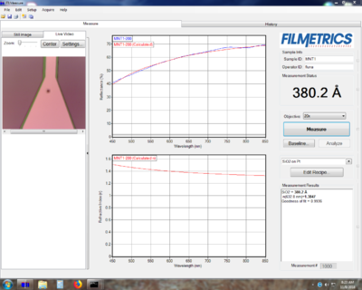
Screenshot showing 10x microscope view and optical spectrum/curve fitting of the SiO2 film thickness on top of Platinum contact metal.
example spectrum curve fit
A good fit should show the Calculated (red) curve overlay on top of the Measureed (blue) curve.
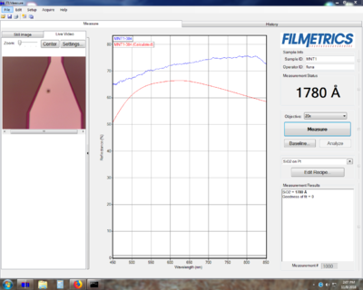
Using the F40-UV to check whether a dry etch is complete.
Example Screenshot of incomplete SiO2 etch
Incomplete Dry-Etch, showing some residual SiO2 left.
Example screenshot of fully removed SiO2 etch
After re-etching, measurement shows bad fit (red and blue curves), indicating the SiO2 film has been fully removed.