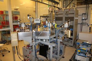
Sputter 2 (SFI Endeavor)
| |||||||||||||||||||||
About
This is a three chamber cluster tool for DC and AC reactive sputtering of metals and dielectrics from 8” cylindrical or 2-piece (for AC) targets. The chamber is configured for 4” diameter wafers or equivalently sized plates that can secure smaller piece samples. Samples are loaded into a cassette system capable of holding 20 wafers. The system is computer controlled through a GUI. Heating of the substrate to several hundred degrees Celcius is possible through a heating lamp module. Chamber 1 is set up for AC reactive sputtering of Al, Al2O3, AlN, SiO2, or SiN. Chamber 2 is set up for DC reactive sputtering of Ti, W, TiN, TiO2, and W-based oxides. Chamber 3 is set up for Al or Au metal sputtering and has RF back-sputtering capability on the sample for sample cleaning prior to deposition.
Detailed Specifications
- Multiple 4” diameter wafer capable system
- Pieces possible through appropriate carrier design
- Full programmable control through GUI
- Heating of substrate to several hundred degrees Celcius
- Chamber 1: AC sputtering of Si, SiN, SiO2, AlN, Al2O3 films
- AlN rate ~ 4.5 nm/min.
- Al2O3 ~ 6 nm/min.
- SiO2 rate ~ 4.5 nm/min.
- Chamber 2: DC sputtering of Ti, TiN, TiO2, W, and W-oxides
- Ti rate ~ 200 nm/min.
- Chamber 3: DC sputtering of Al or Au. RF back-sputtering with Argon
- Al Dep rate ~ 300-400 nm/min.
