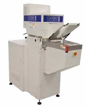
Oxford ICP Etcher (PlasmaPro 100 Cobra)
| ||||||||||||||||||||||||||||||
About
The Oxford PlasmaPro 100 Cobra 300 is intended for etching InP-based, GaAs-baased and GaN-based epitaxies, in addition to Atomic Layer Etching (ALE) processes. The system has a load lock, wide temperature range with rapid heating/cooling, Inductively Coupled Plasma (ICP) coil and a capactively coupled substrate HF (13.56MHz) The fixturing is configured for 4" diameter Si wafers and uses a clamp to hold the sample on the RF chuck. Small pieces may be placed on Silicon carrier wafers, with or without mounting adhesive. Helium back-side cooling is used to keep the sample cool during the etch, but pieces do heat up when placed on carriers.
The in-situ laser monitor installed on this system allows for repeatable etches and endpoint detection via continuous optical monitoring of the wafer reflectivity in a user-determined location, through a porthole on the chamber. The system also has an in situ optical emission monitor for plasma spectroscopy, utilized for chamber clean endpoint detection.
Detailed Specifications
- Temperature Range: –150°C to +400°C
- Gases Available: CH4, H2, Ar, Cl2, BCl3, SF6, SiCl4, O2, N2
- ICP Power (max): 3000 W
- RF Power (max): 600 W
- He-back-side cooling
- 100mm wafer held down with ceramic clamp., single-load
- Users may place pieces onto carrier wafer with or without adhesive. Standard recipes use no adhesive.
- Pieces must be >7mm from edge of carrier to avoid wafer-clamping mechanism.
- Windows-based Cortex software control of process and wafer handling
- Allowed Materials:
- InP-based epitaxies - qualified and ready
- GaAs-baased epitaxies - starter recipe is available
- GaN-based epitaxies - starter recipe is available
- GaSb-based epitaxies - starter recipe is available
- Atomic Layer Etching on select materials - starter recipe is available
- Standard masking materials include:
- SiO2
- Si3N4
- photoresist (at << 100°C).
Other materials can be exposed to the chamber only with staff approval.
- Laser monitoring with camera and etch simulation software: Intellemetrics LEP 500
- Optical Emission Spectroscopy (Ocean Optics) for endpoint detection of chamber cleans & etches - integrated into Oxford software
Documentation
- Oxford PlasmaPro Operating Instructions
- Laser Etch Monitoring procedures
- Online Training Video:
- Oxford Cobra 300 Training
- Important: This video is for reference only, and does not give you authorization to use the tool. You must be officially authorized by the supervisor before using this machine.
Recipes
- Oxford PlasmaPro Recipes - Recipes specific to this tool.
- Process Control Data - Calibration etch data for verifying tool performance over time
- All Dry Etching Recipes - use this list to see other options for dry etching various materials.
