Process Group - Process Control Data
Process Control Data are standardized processes, run by the NanoFab, allowing for day-to-day or year-by-year comparisons of a tool's performance at the process level. This is similar Statistical Process Control (SPC).
These are the same links are found on individual tool pages, in the <<tool page>> > Process Control section.
Data are collected by our Process Group Interns and reviewed by Process Group Staff.
Deposition, Dielectric (Process Control Data)


Process Control data for various deposition tools in the lab.
PECVD #1 (PlasmaTherm 790) - Process Control
PECVD #2 (Advanced Vacuum) - Process Control
ICP-PECVD (Unaxis VLR Dep) - Process Control
- ICP-PECVD: Plots of SiO2 Films
- ICP-PECVD: Plots of Si3N4 Films
- ICP-PECVD: SiO2 Low-Dep Rate (LDR)
- ICP-PECVD: SiO2 High-Dep Rate (HDR)
- ICP-PECVD: Si3N4
- ICP-PECVD: Si3N4 Low-Stress
Ion Beam Sputter Deposition (Veeco Nexus) - Process Control
Old Data (Pre 2022)
Old data in a different format can be found below:
Deposition, Metal - Process Control Data
Process Control data for various deposition tools in the lab.
Sputter 5 (AJA ATC 2200-V) - Process Control
Sputter 5: Ti
Sputter 5: Al
Sputter 5: Cr
E-Beam 4 (CHA) - Process Control
E-Beam 4: Ti
E-Beam 4: Au
E-Beam 4: Cr
E-Beam 4: Ni
E-Beam 1 (Sharon) - Process Control
E-Beam 1: Ti
E-Beam 1: Au
E-Beam 1: Cr
E-Beam 1: Ni
Etching (Process Control Data)
Process Control data for various dry etching tools in the lab.
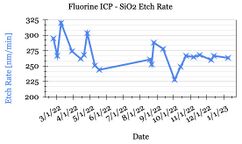
PlasmaTherm SLR Fluorine Etcher - Process Control
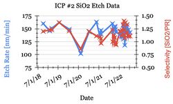
SiO2 Etching (FL-ICP Process Control)
We have found that SiO2 etching is fairly insensitive to chamber condition.
- SiO2 Etching with CHF3/CF4 - Etch Data
- SiO2 Etching with CHF3/CF4 - Plots
Click for Process Control Charts
Old SiO2 Process Control Data
- SiO2 Etching with CHF3/CF4 (FL-ICP) - No data prior to 2023-01-20
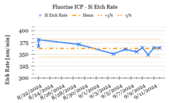
Si Etching (FL-ICP Process Control)
This Si etch is much more sensitive to chamber condition, allowing us to detect chamber contamination faster.
- Recipe: SiVertHFv2 - C4F8/SF6/CF4 etch of 100mm Silicon Wafer with ~50% open area and resist mask
- Si Etching with C4F8/SF6/CF4 - Etch Data
- Si Etching with C4F8/SF6/CF4 - Plots
Click for Process Control Charts
Panasonic ICP #1 - Process Control
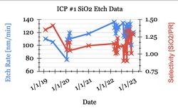
Old Process Control Data
- SiO2 Etch with CHF3/CF4 (Panasonic 1) - No data prior to 2023-01-20
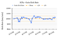
Panasonic ICP#2 - Process Control
GaAs Etch with N2/Cl2 - Process Control Data (Panasonic 2)
SiO2 Etch with CHF3/CF4 - Process Control Data (Panasonic 2)
Old Process Control Data
- SiO2 Etching with CHF3/CF4 - ICP2 - No data prior to 2023-01-20
Unaxis VLR Etch - Process Control
Oxford PlasmaPro Cobra Etcher - Process Control
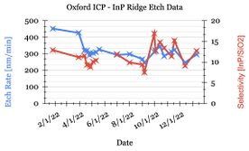
Std InP Ridge Etch Cl2/H2/Ar/200°C
Calibration / Process testing data taken using the "InP Ridge Etch" process: Cl2/H2/Ar @ 200°C, 1cm piece with ~50% SiO2 hardmask.
- "Std InP Ridge Etch" Cl2/H2/Ar 200°C - Etch Data Tables
- "Std InP Ridge Etch" Cl2/H2/Ar 200°C - Plots

Std InP Ridge Etch: Cl2/CH4/H2/60°C
Calibration / Process testing data taken using the "InP Ridge Etch" process: Cl2/CH4/H2 @ 60°C, 1cm piece with ~50% SiO2 hardmask. No longer calibrating this recipe.
- "Std InP Ridge Etch" Cl2/CH4/H2/60°C - Etch Data Tables
- "Std InP Ridge Etch" Cl2/CH4/H2/60°C - Plots
Click for Process Control Charts
Old InP Ridge Etch Data
- InP Ridge Etch with Cl2/CH4/H2 @ 60°C - No data prior to 2023-01-20
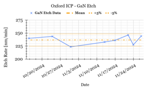
GaN Etch (Cl2/BCl3/Ar/200°C)
Recipe: Std GaN Etch - BCl3/Cl2/Ar - 200C (Public), on 1cm x 1cm ~1.2µm deep GaN etch with Cl2/BCl3/Ar at 200°C. Sapphire substrate with SiO2 mask for GaN.
- GaN Etching with Cl2/BCl3/Ar at 200°C - Etch Data
- GaN Etching with Cl2/BCl3/Ar at 200°C - Plots
Click for Process Control Charts
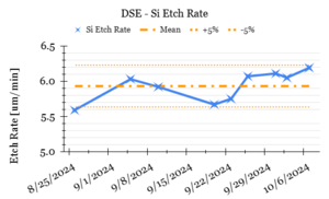
PlasmaTherm DSEIII Deep Silicon Etcher - Process Control
Si Bosch Etching C4F8/SF6/Ar
- Recipe: STD_Bosch_Si (⭐️Production), on 100mm Si Wafer with ~50% open area, photoresist mask, ~40µm deep
- Si Etching with C4F8/SF6/Ar - Etch Data
- Si Etching with C4F8/SF6/Ar - Plots
Click for Process Control Charts
Lithography (Process Control Data)
Process Control Data for Nanofab Lithography/patterning tools.
Stepper #3 (ASML DUV) - Process Control
- The Process Group regularly measures data on lithography Critical Dimension ("CD") and Wafer-stage Particulate Contamination for this tool, using a sensitive lithography process that will reveal small changes in Dose repeatability and wafer flatness.
- Plots of CD Repeatability
- Data for CD Uniformity and Particulate Contamination
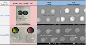
Example of Data Table with SEM's of 320nm features. Click for full data table. 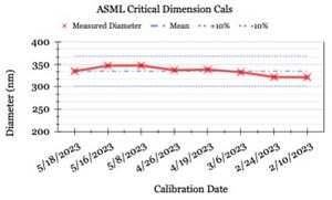
Example SPC Chart - Measured Critical Dimension "CD" versus Date. Click for charts.