ASML Stepper 3 - UCSB Test Reticles
Other Masks and Images
We have various patterns on other plates, such as:
- various line/space,
- alignment markers modifications,
- full-field exposure,
- 1mm boxes
See this document for programming info:
UCSB Masks and Images for ASML
- These are inside the Secure Google Drive folder, you will need to login with your UCSBNetID to access. Ask the Supervisor for access.
- Remember your UCSB NetID is a Google Login, formatted as MyNetID@ucsb.edu. If you are trained on the tool, you already have access using this UCSB NetID login.
Alignment Marks for other systems, other patterns
Reticle ID: "UCSBMARKS26"
This reticle is always installed in the system, in the "System Reticles" Box #1.
Contains many alignment marks, for as many litho systems in the Nanofab as possible. Also edge-bead removal 1cm field, dicing guides, 1mm "boxes" for Laser Monitoring, verniers etc.
See the GDS File & Programming Params in the UCSB Masks Google Drive (login via UCSB NetID)
Other available Images
More patterns can be found on the OAS file and the Excel Sheet of ASML Programming Parameters
(see gDrive folder here - requires UCSB NetID), such as:
- Same alignment marks as above, but with X/Y Vernier alignment measurements
- Layer-2 Vernier (to match the above verniers)
- Dicing guides in X & Y
- ASML PM Marks rotated by 90°, 180° and 270°
- Calibration patterns used in Nanofab LithoCals and EtchCals, such as
- Hex array of holes at 250nm diam / 250nm gap
- Hex array of holes at 400nm diam / 300nm gap (ASML LithoCals)
- 10µm, 1µm, 0.50µm Line/Space (DSE EtchCals)
- Complementary (Layer-2) Alignment Marks for Contact, Inverted marks
Reticle ID: "UCSB-OPC1"
This reticle is always installed in the system, in the "System Reticles" Box #1.
The reticle contains alignment markers for various NanoFab lithography systems, along with resolution test structures and patterns for calibrating optical proximity correction on the system. Some patterns are proprietary to the mask designer, so we can not share the full GDS CAD file.
Alignment Markers
| Image ID | Image Size
X , Y (Wafer, mm) |
Image Shift
X , Y (Wafer, mm) |
Notes/Description | Schematics |
|---|---|---|---|---|
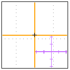
| GCA_Align | 0.530000 , 0.140000 | -6.750000 , 9.450000 | ImageShift references the center of the -X- "global" mark.
The ==||| "Local" mark is X+200µm to the right has 1.1mm margin on all sides |
White is Chrome, Pattern is Clear
|
| JEOL E-Beam Litho Alignment Mark - Positive | 0.900000 , 0.900000 | -6.750000 , -9.450000 | ImageShift is the center coords of the larger "+" mark
Smaller "+" mark is (0.225,-0.225)mm down-right 0.925mm margin on all sides |
White is Chrome, Pattern is Clear |
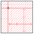
| JEOL E-Beam Litho Alignment Mark - Negative | 0.710000 , 0.710000 | 6.750000 , -9.450000 | ImageShift is the center coords of the larger "+" mark
Smaller "+" mark is (0.225,-0.225)mm down-right Blank (masked) space on left+top sides 1.0mm margin on all sides |
Striped area is Clear |
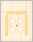
| Contact Mark | 0.564000 , 0.564000 | 6.750000 , 9.450000 | ImageShift references the center of the contact alignment mark "+"
with 1.1mm margin on all sides Note the Polarity - will expose a ~550µm area. |
White is Chrome, Striped area is Clear
CAD File (GDS): Contact-AlignFront.gds Corresponding male/female alignment marks (GDS): MA6-FrontBack_AlignMarks_only.gds |
Resolution Test Charts
The Resolution test charts are repeated all across the reticle, in order to test for lens aberrations. You can have the system expose only a single resolution chart, but since they are placed closely together on the reticle, it's very likely that partial shots of adjacent charts will also be exposed.
In addition, the repeating cells allow us to test for the proper optical proximity correction (OPC) algorithm. The Five Dense_... patterns are for calibrating the OPC algorithm, and are not for user analysis.
Patterned area is CLEAR/transparent.
Calibration Chart Layout
Cell name is "UCSB_Cal", with coordinates below pointing to center of this cell.
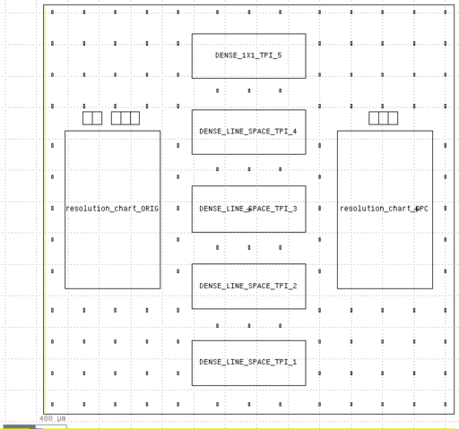
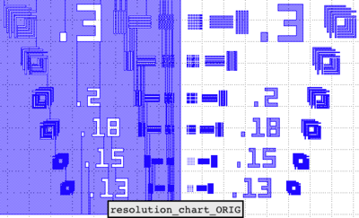
Resolution Chart
"resolution_chart_ORIG" cell in the above. Blue/patterned area is CLEAR/transparent.
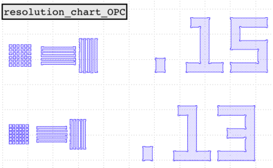
The ""resolution_chart_OPC" version has an optical proximity correction algorithm applied:
Coords for "resolution_chart" Calibration patterns
Image coords for each of the "resolution_chart_ORIG" cells. You can pick just one of these for shooting a resolution test structure. The purpose of the many different locations is to check for variations due to lens aberrations. You could just choose one near the center of the plate to test your process, or you could choose a chart that is in a similar location as the pattern you're shooting on your mask plate.
Note that some portion of the adjacent patterns will likely be exposed as well, due to the patterns not being surrounded by 1mm of chrome. Make sure you set your Cell Size large enough to make sure the bleed-over doesn't overlap with adjacent die.
| Image Size
X , Y (Wafer, mm) |
Image Shift
X (Wafer, mm) |
Image Shift
Y (Wafer, mm) |
|---|---|---|
| Use this for a single Resolution Chart: | ||
| 0.605 , 1.005 | 0.685000 | 1.350000 |
| The following are Res Charts across the exposure field: | ||
| 0.605 , 1.005 | -10.115000 | 12.150000 |
| same for each | -7.415000 | 12.150000 |
| " " | -4.715000 | 12.150000 |
| " " | -2.015000 | 12.150000 |
| " " | 0.685000 | 12.150000 |
| " " | 3.385000 | 12.150000 |
| " " | 6.085000 | 12.150000 |
| " " | 8.785000 | 12.150000 |
| -10.115000 | 9.450000 | |
| Alignment Marker | ||
| -4.715000 | 9.450000 | |
| -2.015000 | 9.450000 | |
| 0.685000 | 9.450000 | |
| 3.385000 | 9.450000 | |
| Alignment Marker | ||
| 8.785000 | 9.450000 | |
| -10.115000 | 6.750000 | |
| -7.415000 | 6.750000 | |
| -4.715000 | 6.750000 | |
| -2.015000 | 6.750000 | |
| 0.685000 | 6.750000 | |
| 3.385000 | 6.750000 | |
| 6.085000 | 6.750000 | |
| 8.785000 | 6.750000 | |
| -10.115000 | 4.050000 | |
| -7.415000 | 4.050000 | |
| -4.715000 | 4.050000 | |
| -2.015000 | 4.050000 | |
| 0.685000 | 4.050000 | |
| 3.385000 | 4.050000 | |
| 6.085000 | 4.050000 | |
| 8.785000 | 4.050000 | |
| -10.115000 | 1.350000 | |
| -7.415000 | 1.350000 | |
| -4.715000 | 1.350000 | |
| -2.015000 | 1.350000 | |
| 0.685000 | 1.350000 | |
| 3.385000 | 1.350000 | |
| 6.085000 | 1.350000 | |
| 8.785000 | 1.350000 | |
| -10.115000 | -1.350000 | |
| -7.415000 | -1.350000 | |
| -4.715000 | -1.350000 | |
| -2.015000 | -1.350000 | |
| 0.685000 | -1.350000 | |
| 3.385000 | -1.350000 | |
| 6.085000 | -1.350000 | |
| 8.785000 | -1.350000 | |
| -10.115000 | -4.050000 | |
| -7.415000 | -4.050000 | |
| -4.715000 | -4.050000 | |
| -2.015000 | -4.050000 | |
| 0.685000 | -4.050000 | |
| 3.385000 | -4.050000 | |
| 6.085000 | -4.050000 | |
| 8.785000 | -4.050000 | |
| -10.115000 | -6.750000 | |
| -7.415000 | -6.750000 | |
| -4.715000 | -6.750000 | |
| -2.015000 | -6.750000 | |
| 0.685000 | -6.750000 | |
| 3.385000 | -6.750000 | |
| 6.085000 | -6.750000 | |
| 8.785000 | -6.750000 | |
| -10.115000 | -9.450000 | |
| Alignment Marker | ||
| -4.715000 | -9.450000 | |
| -2.015000 | -9.450000 | |
| 0.685000 | -9.450000 | |
| 3.385000 | -9.450000 | |
| Alignment Marker | ||
| 8.785000 | -9.450000 | |
| -10.115000 | -12.150000 | |
| -7.415000 | -12.150000 | |
| -4.715000 | -12.150000 | |
| -2.015000 | -12.150000 | |
| 0.685000 | -12.150000 | |
| 3.385000 | -12.150000 | |
| 6.085000 | -12.150000 | |
| 8.785000 | -12.150000 | |
Coords for "UCSB_Cal" Calibration Patterns
Each of the above "UCSB_Cal" cells, including all 7 patterns, is repeated on the following coordinates across the plate (coords are to the center of the "UCSB_Cal" cell):
| Image Size
X , Y (Wafer, mm) |
Image Shift
X (Wafer, mm) |
Image Shift
Y (Wafer, mm) |
|---|---|---|
| 2.610000 , 2.610000 | -9.450000 | 12.150000 |
| same as above | -6.750000 | 12.150000 |
| " " | -4.050000 | 12.150000 |
| " " | -1.350000 | 12.150000 |
| " " | 1.350000 | 12.150000 |
| " " | 4.050000 | 12.150000 |
| " " | 6.750000 | 12.150000 |
| " " | 9.450000 | 12.150000 |
| -9.450000 | 9.450000 | |
| Alignment Marker | ||
| -4.050000 | 9.450000 | |
| -1.350000 | 9.450000 | |
| 1.350000 | 9.450000 | |
| 4.050000 | 9.450000 | |
| Alignment Marker | ||
| 9.450000 | 9.450000 | |
| -9.450000 | 6.750000 | |
| -6.750000 | 6.750000 | |
| -4.050000 | 6.750000 | |
| -1.350000 | 6.750000 | |
| 1.350000 | 6.750000 | |
| 4.050000 | 6.750000 | |
| 6.750000 | 6.750000 | |
| 9.450000 | 6.750000 | |
| -9.450000 | 4.050000 | |
| -6.750000 | 4.050000 | |
| -4.050000 | 4.050000 | |
| -1.350000 | 4.050000 | |
| 1.350000 | 4.050000 | |
| 4.050000 | 4.050000 | |
| 6.750000 | 4.050000 | |
| 9.450000 | 4.050000 | |
| -9.450000 | 1.350000 | |
| -6.750000 | 1.350000 | |
| -4.050000 | 1.350000 | |
| -1.350000 | 1.350000 | |
| 1.350000 | 1.350000 | |
| 4.050000 | 1.350000 | |
| 6.750000 | 1.350000 | |
| 9.450000 | 1.350000 | |
| -9.450000 | -1.350000 | |
| -6.750000 | -1.350000 | |
| -4.050000 | -1.350000 | |
| -1.350000 | -1.350000 | |
| 1.350000 | -1.350000 | |
| 4.050000 | -1.350000 | |
| 6.750000 | -1.350000 | |
| 9.450000 | -1.350000 | |
| -9.450000 | -4.050000 | |
| -6.750000 | -4.050000 | |
| -4.050000 | -4.050000 | |
| -1.350000 | -4.050000 | |
| 1.350000 | -4.050000 | |
| 4.050000 | -4.050000 | |
| 6.750000 | -4.050000 | |
| 9.450000 | -4.050000 | |
| -9.450000 | -6.750000 | |
| -6.750000 | -6.750000 | |
| -4.050000 | -6.750000 | |
| -1.350000 | -6.750000 | |
| 1.350000 | -6.750000 | |
| 4.050000 | -6.750000 | |
| 6.750000 | -6.750000 | |
| 9.450000 | -6.750000 | |
| -9.450000 | -9.450000 | |
| Alignment Marker | ||
| -4.050000 | -9.450000 | |
| -1.350000 | -9.450000 | |
| 1.350000 | -9.450000 | |
| 4.050000 | -9.450000 | |
| Alignment Marker | ||
| 9.450000 | -9.450000 | |
| -9.450000 | -12.150000 | |
| -6.750000 | -12.150000 | |
| -4.050000 | -12.150000 | |
| -1.350000 | -12.150000 | |
| 1.350000 | -12.150000 | |
| 4.050000 | -12.150000 | |
| 6.750000 | -12.150000 | |
| 9.450000 | -12.150000 | |
