ASML Stepper 3 Standard Operating Procedure
Regular Procedures for ASML Deep-UV Stepper #3
Normal User Procedures
- BEFORE starting your job, check the Warnings window for any errors, and deal with them first.
- You may need to press the [F4] Front keyboard key to bring the window forward.
- See the "Errors: Warnings" section for how to deal with these.
- BEFORE starting your job, check the Warnings window for any errors, and deal with them first.
- Cleaning the back-sides of wafers: Very important
- Make sure all work surfaces/spin chucks/hot plates are cleaned! Don’t use wipes, place baked wafers directly on cleaned steel surfaces.
- Cleaning residue of DUV42P or DSK101 (BARC’s): This technique is much better than trying to wipe. Use clean gloves and hold the wafer edges with your hands.
- After spin coating, BEFORE baking, place wafer upside down in POLOS spinner using non-contact chuck.
- Set spin speed to 2000rpm. Program “backside”.
- Spin wafer, wait until at top speed.
- Squirt “Remover PG” 10sec, then Acetone 3 seconds, then ISO for 3 sec.
- Spin Dry while blowing with N2. Wait ~5sec before stopping spin.
- Remove wafer and do bake as normal.
- Cleaning residues of DUV PR’s such as: UV210, UV6, UVN2300:
- After baking, place wafer face-down in POLOS spinner using non-contact chuck.
- Set spin speed to 2000rpm. Program “backside”
- Spin wafer, wait until at top speed.
- Squirt Acetone on sample back for 3 seconds. Followed by ISO for 3 sec.
- Spin Dry while blowing with N2.
- Bring wafers and ASML cassette to Solvent bench, ensure surfaces are clean from solvents.
- Check back-side of wafer thoroughly for particulates before loading into system! If you see particulates, try to blow then off with high N2 flow first. You may need to get physical with a razor blade to remove stubborn particles.
- Do this in the solvent bench where HEPA filters keep the air cleaner.
- Reticle Unloading and Loading
- (Mat Hdl) Material Handler (button near top right of software window)
- Remove reticles from machine
- Exchange reticle box
- Unlock box3
- Physically Remove desired reticle pod(s), green “3” indicator at box should be lit and all reticles should be lifted up into pod.
- Use manual box opener to open reticle box. Move arm slowly.
- Remove Pod Lid
- Remove (or add) reticle to pod.
- Two stars on reticle should be in front
- Chrome (dark) side down
- Place Pod lid back on
- Close Pod using arm, move arm slowly
- Place Pod back in stepper
- Read desired pods
- Go back to main menu once mask barcodes are all showing on screen
- (Mat Hdl) Material Handler (button near top right of software window)
- Wafer Load
- Open lid, Remove cassette
- (make sure backs of wafers are extremely clean! No Particles! No residues! Be extra careful and attentive to this detail! See above cleaning procedure)
- Place wafers in slots
- Place cassette back. Make sure cassette is pulled back snugly in place
- Close Lid.
- Running a Job – Normal operation
- Batch Control > Task Streaming
- Wait until wafers are read by machine
- Task: Batch > (Append)
- Enter Batch ID first, Hit Return to apply change
- Press Select Button under Job Name and navigate to your job
- Click on Layer ID to get a list of layers you can expose: Select layer you want
- Enter number of wafers in Batch Size
- Batch Type is “P” for production run (see below for doing a FEM)
- Verify Energy, Focus Offset, Ilumination Mode, NA, Sigma and change as desired
- Hit Action > (Apply) button to register all changes
- Press (Accept) Button at Top
- Press Queue > (Continue) Button to execute batch.
- If Batch has general failure:
- Click the (HELP) button on error window and photograph the error chain - send to supervisor if needed.
- Choose “clear litho cluster” option to remove all wafers to output Port.
Running a focus and/or exposure matrix
Focus-Exposure Matrix/Arrays (FEM or FEA) are used to determine the proper exposure dose & focus offset for your lithography. Especially important for high-resolution layers. Make sure your entire litho process remains constant (spins, bakes, develop times etc.) between the FEA and your real sample lithos.
- Optional: Copy you job to a new job file with the layers/images you want to shoot, but which does not fill the entire wafer to the edges - it instead has only a ~6x6-cm wide array of die (set in the Wafer Layout > Image Distribution section of your program). This ensures that our SEMs can view the full array (The extreme edges of a 4-inch wafer are not possible to image on our SEMs due to motor limits) and simplifies calculations while inspecting the exposed wafer.
- Follow "Running a Job" procedure above, until Step 7
- Under Batch Type:
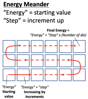
- Choose E for exposure snake (with flat down, first exposure lower left increments to the right, snakes in serpentine manner around entire wafer). Enter starting exposure in mJ (bottom-left die) and incremental exposure in mJ (increments up).
- Choose F for focus snake (with flat down, first exposure lower left increments to the right, snakes around entire array). Enter starting focus offset (bottom-left die) and incremental focus for the snake (increments up).
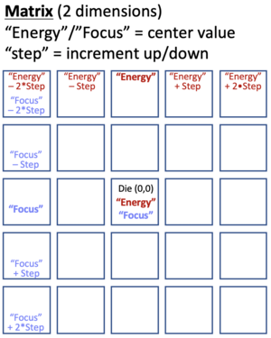
- Choose M for Focus-Exposure-Matrix (FEM). Center cell 0,0 is the nominal Exposure Energy and Focus value you enter. The array is incremented up and down from the nominal value. By default, exposure Energy varies by columns, Focus by Rows. See schematic below.
- Verify non-varied parameters as well as Ilumination Mode, NA, Sigma and change as desired.
- Hit Action: (Apply) button to register all changes
- Check ALL the Images in the job! Use the (Preset) button to apply to all Images in the job.
- Press Accept Button at Top
- (optional) Before running the exposure, click Batch: (Report) to view the exposure (dose/focus) distribution.
- If you need to alter the FEM, close the report and choose Batch: (Modify) and "Overwrite report" when prompted.
- Press Continue Button to execute batch.
- When the batch is complete, select the batch in the Task ist, and click Batch: (Report). The "Test Exposure Data" section of the report shows the exposure params for each die location. This is very useful during your inspection, and it is recommended that you bring a photograph or copy of this exposure matrix table with you when inspecting on the microscope/SEM.
FEM Array/Matrix Layout
The below schematics show how the ASML PAS software arranges the varying Dose/Focus on a wafer. The layout is always calculated with respect to with the Cell at Column/Row = (0,0) in your program's Cell Layout.
 |
 |
|---|
Tips for FEM analysis
- Tutorial: Analyzing a Focus-Exposure Matrix (FEM) - New detailed tutorial on how to optimize your litho, the brief summary is below:
You need to find the center of the Viable Process Window - meaning you need to see the BAD dose (too high + too low) and BAD focus (too high + too low) then choose a Dose+Focus in the middle of this range. This allows your process to work even if the focus or some other process varies.
You'll need to decide what "good enough" looks like on your feature inspection - this is your process tolerance. For example instead of looking for "the feature that is exactly 300nm wide", you may want to look for Dose/Focus where "the feature is between 250-350nm, or 300nm±50nm". Thus your process has a viable tolerance to normal fabrication variations. You may want to run simulations or other estimates for what the tolerance may be.
A common mistake is to look for "the best die" - but this one good die could be (and often is) at the edge of the working process window, so a small process variation (wafer thickness, hotplate temperature) will put your process outside the process window - you'll have chosen a very tight process that easily goes out of spec with random fluctuation in the process.
General process:
- Run a "Coarse" (wide-range) Focus-Exposure Matrix using the "starting params" from the wiki for your PR/tool.
- Analyze (microscope or SEM) to find the edges of the process window in both Focus & Dose. Often this can be done somewhat fast by eye and optical microscope, without detailed measurements, allowing you to locate the center of the process window based on the obviously "Bad" rows/cols.
- Tip: If possible, mark up your wafer with sharpie, scribes or other to make the grid easier to analyze, especially to avoid getting "lost" on the SEM.
- Run a "Fine" FEM with finer step size.
- On the ASML, you can now keep the Focus constant according to the central Focus value from your Coarse FEM, and do only an Energy serpentine.
- Analyze to measure actual feature size, according to your process tolerance.
Written by: Demis D. John, original operating procedure written by Brian Thibeault & Adam Abrahamson.