PECVD-2 - a-Si Recipe and Dep process (2025)
Jump to navigation
Jump to search
Developed by Ryan Hersey & Skyler Palatnik, from the research group of Prof. Max Millar-Blanchaer. Nov. 2025
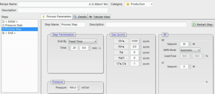
- Recipe Name: ★ A Si 900mT RH
- Dep Rate: ~5.5nm/min
- Stress: -700MPa
- n(1600nm) ≈ 3.68
- High uniformity for a single 100mm wafer.
Process Flow:
- (optional) wet clean
- 5min coat
- Max 60min dep before breaking it up and cleaning the chamber.
- Wet-Clean chamber walls
- Dry Clean: 2min std. clean per 1min a-Si dep.
Do not modify this recipe with discussing with Staff first (eg. Tool Supervisor), as mods usually require altering the dry clean times as well.
Recipe Parameters

Recipe Params:
- 300°C
- 900mT
- SiH4 = 1500 sccm
- 30W (HF)