Stepper Reticle Layout (Advanced) - Complex Experiments and Variations
Example CAD Files
- CAD_Tutorial_for_ASML_Reticle_v2_DEMIS-DOE.OAS - example CAD file for reticle with many design variations.
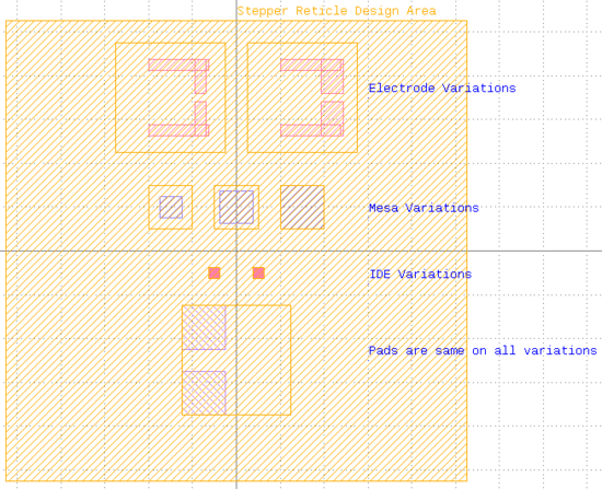
- Cell "Reticle_Layout" shows the mask that would be printed by a photomask vendor. You would print Layers 1,2 and 3 onto a single mask plate, with the CAD file origin at the center of the mask plate (no automatic centering).
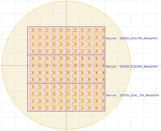
- Cell "Wafer_Layout" shows an estimation/"simulation" of design variations to be exposed on the wafer. It is only a "simulation" because the real layout would be programmed on the Stepper tool itself, which may make changes (such as automatically filling to the wafer's edge).
- ASML_Reticle_Programming_Params_-_DEMIS-DOE_v1.xlsx - stepper programming sheet for the above CAD file, for typing in the mask's Images into the Stepper software.
Reticle Layout

- Setup your reticle with separate Images, each Image corresponding to a design variation.
- In the example below, my mask plate has the following design variations:
- Electrode Width: 2 variations (1mm wide, 500µm wide)
- Mesa Width: 3 variations (500µm, 750µm, 1000µm)
- Interdigitated Electrodes with Line/Space variations (250nm and 350nm)
- A single Pad Layer design, that works for any device variation.
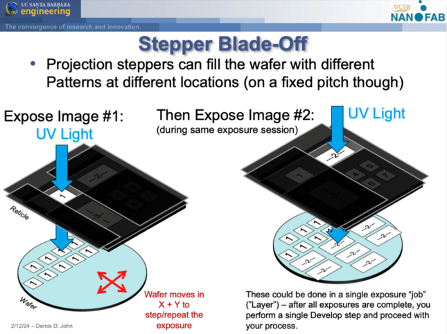
Since these Images are setup with enough opaque Chrome between them that the Stepper can block off and select a single Image for exposure, we can program the stepper to mix & match any design variation across my wafer.
| Reticle with design variations |
|---|
| Example reticle with rows of different design variations.
Note the spacing between each Image should be opaque chrome, and wide enough for the stepper shutters/blades - see the parameters on each stepper's Mask Making Guidelines page. |
Stepper Job Programming
The KLayout simulated wafer layout below would actually have to be programmed in the Stepper's exposure Job, as follows:
- The Top 1/3 of the Wafer gets:
- Layer 1 = IDE 250nm line/space
- Layer 2 = Mesa 2000µm
- Layer 3 = Electrodes = 750µm
- Layer 4 = Standard Pads Image.
- The Middle 1/3 of the Wafer gets:
- Layer 1 = IDE 350nm line/space
- Layer 2 = Mesa 1000µm
- Layer 3 = Electrodes = 500µm
- Layer 4 = Standard Pads Image.
- The Bottom 1/3 of the Wafer gets:
- Layer 1 = IDE 350nm line/space
- Layer 2 = Mesa 2000µm
- Layer 3 = Electrodes = 750µm
- Layer 4 = Standard Pads Image.
| Simulated wafer layout picking from different designs |
|---|
| This would actually need to be programmed on the Stepper, this KLayout schematic is just a "simulation". |
Exposures during processing
When you actually run the wafers, each Lithography will automatically pattern the variations you have setup; you will do your lithography as follows:
- Layer 1 (IDE) will expose:
- Top 1/3 of the Wafer: IDE 250nm line/space
- Middle 1/3 of the Wafer: IDE 350nm line/space
- Bottom 1/3 of the Wafer: IDE 350nm line/space
Then you perform your liftoff or etch etc. Then you perform the next litho as follows:
- Layer 2 (Mesa) will expose:
- Top 1/3 of the Wafer: Mesa 2000µm
- Middle 1/3 of the Wafer: Mesa 1000µm
- Bottom 1/3 of the Wafer: Mesa 2000µm
You perform your Mesa etch, and then run Layer 3 exposure which does the following:
- Layer 3 (Electrodes) will expose:
- Top 1/3 of the Wafer: Electrodes = 750µm
- Middle 1/3 of the Wafer: Electrodes = 500µm
- Bottom 1/3 of the Wafer: Electrodes = 750µm
And the final Layer "pads" will expose the same Pads Image on every die, then you can perform a single develop & evaporation & liftoff to complete all the devices.

