Stepper Mask-Making Guidelines (Generic)
Jump to navigation
Jump to search
Generic Stepper Mask Parameters
Tutorial: If you are not familiar with the difference between designing Contact Litho Masks and Stepper Litho Masks/Reticles, please review this short tutorial:
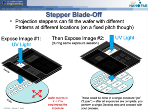
For the stepper you are designing for, make sure you know:
- The maximum exposure field size, and
- The minimum gap between adjacent patterns/images that must be dark chrome (for the system's reticle shutters to block adjacent images)
- Either the quoted product number from our photomask vendor quotes, or reticle size/thickness/material (eg. 5" x 5" x 0.090", Soda-Lime glass)
These values will vary depending on the stepper you're designing for. Contact the Stepper's Process Expert or Tool Supervisor to find out these values.
Generic Stepper design/programming CAD files & spreadsheets
- Example Toppan Order Form via Digidat
- Academic users may request the UCSB Nanofab's quotes from various photomask vendors.
- Fill out this Spreadsheet before programming your job on the machine, using your CAD file:
- UCSB_Stepper_-_Programming_Worksheet.pptx - New version of the spreadsheet below, that also includes the wafer-layout info needed to generate a basic stepper exposure program.
- Stepper Reticle Programming Params - MASKJAN2020 v1.xlsx (example for fictional barcode "MASKJAN2020") - Spreadsheet form of the above PPT. Faster to fill out for "expert" stepper users.
- On-wafer alignment marks:
- This pattern is usually available on a system reticle - you are not required to include the alignment mark pattern in your own designs.
- Please check for the specific Stepper you are using.
Example CAD File and Programming
Using an Example CAD file, here is the corresponding Mask Order Form & Spreadsheet:
- Example CAD file from Utilities > CAD Layout > Example CAD File, designed in KLayout.
- Example "Stepper Reticle Programming Params" spreadsheet for reticle "DEM-2020-03"
- Example Reticle Order Form for reticle "DEM-2020-03"
CAD Tips
- By default, Wafer flat is Down (–Y) with respect to your CAD file.
- Utilize the "Cell" and "Cell Instancing" functionality in your CAD layout program! (aka. a "Block" in AutoCAD). Highly recommended to use KLayout, not AutoCAD. See Calculators + Utilities > CAD Design Tips for tutorials.
- Center your entire design around the coordinates (0,0). (0,0) should always be the center of your device, wafer and/or photomask/reticle. Photomask vendors should then NOT "auto center" your designs on the plate.
- Inside each sub-Cell, also design around the cell's (0,0) origin.
- Create a Cell called "reticle_layout" or similar, that is an exact representation of what the printed reticle patterns should look like (typically at 1x wafer-scale, if not including the outer templates for the stepper system). Instance the Device's Cells into reticle_layout, and reference this Cell on your mask order form. (You can also Instance the same cells into "device_layout" and "wafer_layout" cells during design/verification.)
If you follow the above rules, your printed "reticle_layout" Cell will have Instances of each of your design's Images/patterns, and the coordinates/sizes of these Cells are exactly what you use to write your Stepper program.
See the example CAD Files here: