Surface Analysis (KLA/Tencor Surfscan): Difference between revisions
Jump to navigation
Jump to search
Content deleted Content added
→Documentation: wafer scanning process traveler |
|||
| Line 18: | Line 18: | ||
**''For detailed measurement info, it is highly recommended that you read the manual.'' |
**''For detailed measurement info, it is highly recommended that you read the manual.'' |
||
*[//wiki.nanotech.ucsb.edu/w/images/2/27/Surfscan-Surfscan_6200_info.pdf Surfscan Info] |
*[//wiki.nanotech.ucsb.edu/w/images/2/27/Surfscan-Surfscan_6200_info.pdf Surfscan Info] |
||
*Wafer scanning process traveler |
|||
* |
* |
||
=== Screenshots === |
=== Screenshots === |
||
Revision as of 22:19, 31 March 2020
|
About
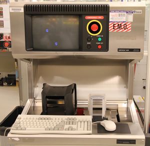
This system uses a laser-based scattering method to count size and distribution of particles (or other scattering defects) on a flat wafer surface. It can scan wafers in size from 4 to 8 inches.
Documentation
- Standard Operating Procedure
- Operations Manual
- For detailed measurement info, it is highly recommended that you read the manual.
- Surfscan Info
- Wafer scanning process traveler
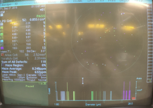
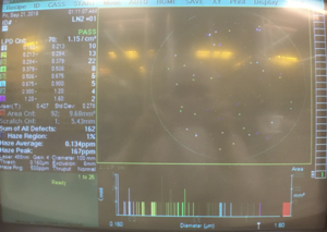
Screenshots


