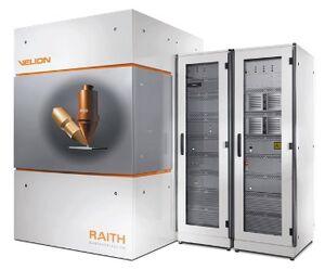
Focused Ion-Beam Lithography (Raith Velion): Difference between revisions
Jump to navigation
Jump to search
Content deleted Content added
m →Recipes: formatting |
|||
| Line 12: | Line 12: | ||
}} |
}} |
||
= About = |
= About = |
||
The |
The Raith Velion ion beam tool was installed at UCSB in 2020 and signed off and avaiable for. use in early 2021. |
||
This system uses the vector scan approach for electron beam deflection within a field, step and repeat for stage movement between fields, the combination of which allows the entire area of the sample to be exposed to the electron beam. |
This system uses the vector scan approach for electron beam deflection within a field, step and repeat for stage movement between fields, the combination of which allows the entire area of the sample to be exposed to the electron beam. |
||
| Line 19: | Line 19: | ||
=Detailed Specifications= |
=Detailed Specifications= |
||
*Utilizes a “Hi-brightness” thermal field emission electron source (ZnO/W) with a minimum spot-size at the substrate of 2nm; operates at 100kV only |
|||
*Unique two lens/deflector scanning system: |
|||
**<u>4th lens</u> => 20-25nm minimum line-width, 1.000nm scan step resolution, 500 x 500um scan field |
|||
**<u>5th lens</u> => 7-8 nm minimum line-width, 0.125nm scan step resolution, 62.5x62.5um scan field |
|||
*Maximum deflector scan speed = 25MHz (=> 40ns/pixel minimum dwell time) |
|||
*150x150 mm writable area; stage position control to 0.6nm accuracy (λ/1024); 10mm/s maximum stage speed |
|||
*Dynamic Focus and Stigmation Control for improved writing performance across the entire scan field. |
|||
*UNIX computer controlled |
|||
*Advanced Fracturing software available (Layout BEAMER from GeniSys, Inc) |
|||
** automated proximity correction of patterns possible |
|||
** ability to manually position write fields within a pattern for optimum inter-field writing performance |
|||
** ability to adjust beam scanning strategy within a write field for optimum intra-field writing performance |
|||
** fine tuning of line-edge roughness by shot pitch correction |
|||
nanoFIB column: |
|||
* Liquid Metal Alloy Ion Sources (LMAIS) providing ions for Gallium-free patterning (Au, Si) |
|||
* High resolution patterning capabilities (minimum feature size < 15nm) |
|||
* Fully corrected write fields (distortion, stigmation) |
|||
* Long term current stability (days) |
|||
Laser Interferometer stage: |
|||
* Mechanical movement at 1nm precision |
|||
* Continuous stage modes for stitch free FIB patterning on full 4”wafer scale |
|||
* Stitching and overlay accuracy: < 50 nm ( mean+3 sigma) |
|||
FE SEM |
|||
* Process control for rapid prototyping |
|||
Additional Capabilities: |
|||
* Automated height sensing to detect sample surface height variation for automated correction |
|||
* Pt Gas Iinjection System (GIS) deposition |
|||
* |
|||
* Raith Nanosuite software incl. CAD (GDSII) navigation & patterning |
|||
== Recipes == |
== Recipes == |
||
* Recipes > Lithography > '''[[Lithography Recipes#FIB Lithography Recipes .28Raith Velion.29|<u>FIB Lithography</u>]]''' |
* Recipes > Lithography > '''[[Lithography Recipes#FIB Lithography Recipes .28Raith Velion.29|<u>FIB Lithography</u>]]''' |
||
Revision as of 14:48, 12 March 2021
 Work In Progress This article is still under construction. It may contain factual errors. Content is subject to change. |
|
About
The Raith Velion ion beam tool was installed at UCSB in 2020 and signed off and avaiable for. use in early 2021.
This system uses the vector scan approach for electron beam deflection within a field, step and repeat for stage movement between fields, the combination of which allows the entire area of the sample to be exposed to the electron beam.
The machine can be run at 25, 50 and 100 kV. Note however that only the 100kV mode is used at UCSB.
Detailed Specifications
nanoFIB column:
- Liquid Metal Alloy Ion Sources (LMAIS) providing ions for Gallium-free patterning (Au, Si)
- High resolution patterning capabilities (minimum feature size < 15nm)
- Fully corrected write fields (distortion, stigmation)
- Long term current stability (days)
Laser Interferometer stage:
- Mechanical movement at 1nm precision
- Continuous stage modes for stitch free FIB patterning on full 4”wafer scale
- Stitching and overlay accuracy: < 50 nm ( mean+3 sigma)
FE SEM
- Process control for rapid prototyping
Additional Capabilities:
- Automated height sensing to detect sample surface height variation for automated correction
- Pt Gas Iinjection System (GIS) deposition
- Raith Nanosuite software incl. CAD (GDSII) navigation & patterning
Recipes
- Recipes > Lithography > FIB Lithography
- Contains starting recipes etc.
