Optical Film Thickness (Nanometric): Difference between revisions
No edit summary |
(Note stating tool removed from lab.) |
||
| Line 9: | Line 9: | ||
|manufacturer = Nanometrics |
|manufacturer = Nanometrics |
||
|materials = |
|materials = |
||
}} |
}} |
||
| ⚫ | |||
<code>'''This tool is currently unavailable - Tool Removed from lab due to low usage on 2022-03-22'''</code> |
|||
| ⚫ | |||
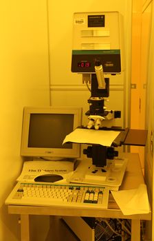
This tool is for thickness and optical property measurements of films on silicon substrates. Other substrates are permitted, but results will not be accurate. The technique used is white light reflection. Data is taken with normal incidence reflection of white light (480 nm – 850 nm) from the surface and spectral data is captured through a spectrometer attached to the camera port of the microscope. The data is modeled and the optical parameters are adjusted to give a best least-squared fit to the data. Refractive index can be manually entered or used as a parameter in the fitting routine. Absorbing films will give incorrect results. This unit can measure thicknesses of films in spots down to approximately 10 um, allowing for measurement of thin films at various points in the processing. |
This tool is for thickness and optical property measurements of films on silicon substrates. Other substrates are permitted, but results will not be accurate. The technique used is white light reflection. Data is taken with normal incidence reflection of white light (480 nm – 850 nm) from the surface and spectral data is captured through a spectrometer attached to the camera port of the microscope. The data is modeled and the optical parameters are adjusted to give a best least-squared fit to the data. Refractive index can be manually entered or used as a parameter in the fitting routine. Absorbing films will give incorrect results. This unit can measure thicknesses of films in spots down to approximately 10 um, allowing for measurement of thin films at various points in the processing. |
||
=Equipment Specifications= |
=Equipment Specifications= |
||
*480-850 nm reflection spectrum |
*480-850 nm reflection spectrum |
||
*Designed for silicon substrates; others allowed, but accuracy not guaranteed |
*Designed for silicon substrates; others allowed, but accuracy not guaranteed |
||
Revision as of 17:59, 22 March 2022
|
This tool is currently unavailable - Tool Removed from lab due to low usage on 2022-03-22
About
This tool is for thickness and optical property measurements of films on silicon substrates. Other substrates are permitted, but results will not be accurate. The technique used is white light reflection. Data is taken with normal incidence reflection of white light (480 nm – 850 nm) from the surface and spectral data is captured through a spectrometer attached to the camera port of the microscope. The data is modeled and the optical parameters are adjusted to give a best least-squared fit to the data. Refractive index can be manually entered or used as a parameter in the fitting routine. Absorbing films will give incorrect results. This unit can measure thicknesses of films in spots down to approximately 10 um, allowing for measurement of thin films at various points in the processing.
Equipment Specifications
- 480-850 nm reflection spectrum
- Designed for silicon substrates; others allowed, but accuracy not guaranteed
- 150 A to tens of microns thickness measurements
- Do not use refractive index option for very thin films
- Manual wafer placement, up to 6" wafers
- Objectives of 5x, 10x, and 20x for 40 um, 20 um, and 10 um spot sizes.; can measure film properties in small areas
- Thicker films require lower objective magnification due to depth of focus
- Programs for PR, SiO2, SiN on silicon
