Mechanical Polisher (Allied): Difference between revisions
Jump to navigation
Jump to search
Content deleted Content added
update to {{tool2}}, set Room = 1111 |
Millerski w (talk | contribs) Added SOP Link |
||
| Line 10: | Line 10: | ||
|toolid=70 |
|toolid=70 |
||
}} |
}} |
||
= |
=About= |
||
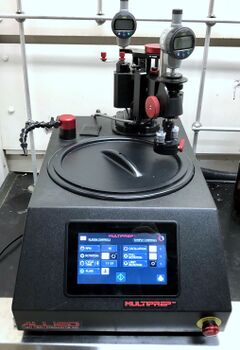
The Allied Polisher allows for bulk thinning of substrates, and fine polishing of optical waveguide facets. Various materials are typically lapped/polished, such as Silicon GaAs, InP. |
The Allied Polisher allows for bulk thinning of substrates, and fine polishing of optical waveguide facets. Various materials are typically lapped/polished, such as Silicon GaAs, InP. |
||
== |
==Detailed Specs== |
||
| ⚫ | |||
| ⚫ | |||
| ⚫ | |||
| ⚫ | |||
| ⚫ | |||
| ⚫ | |||
| ⚫ | |||
| ⚫ | |||
== Operating Procedures == |
|||
| ⚫ | |||
| ⚫ | |||
| ⚫ | |||
| ⚫ | |||
| ⚫ | |||
| ⚫ | |||
| ⚫ | |||
== |
==Operating Procedures== |
||
* ''To Be Added'' |
|||
*[https://wiki.nanotech.ucsb.edu/w/images/f/f2/Mechanical_Polisher_SOP_Rev_A.pdf Mechanical Polisher SOP] |
|||
==Recipes== |
|||
| ⚫ | |||
Latest revision as of 16:06, 15 May 2023
| ||||||||||||||||||||||||||||
About
The Allied Polisher allows for bulk thinning of substrates, and fine polishing of optical waveguide facets. Various materials are typically lapped/polished, such as Silicon GaAs, InP.
Detailed Specs
- Max. Substrate Size
- Lapping Films available:
- 10µm AlOx
- 5µm AlOx
- 2µm AlOx
- 1µm AlOx
- 0.5 AlOx
Operating Procedures
Recipes
- To Be Added
