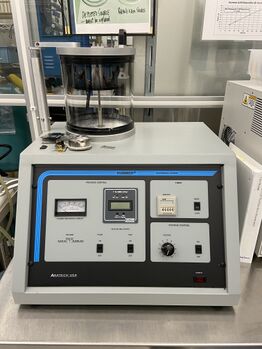
SEM Sample Coater (Hummer): Difference between revisions
Jump to navigation
Jump to search
Content deleted Content added
Instructions |
→Operating Procedures: fixed bullet points, listed approx film thickness |
||
| (One intermediate revision by the same user not shown) | |||
| Line 11: | Line 11: | ||
}} |
}} |
||
=About= |
=About= |
||
This system is for coating |
This system is for coating thin (1-10nm) AuPd layers onto samples that will reduce charging during FESEM inspection. |
||
===When to use=== |
===When to use=== |
||
| Line 18: | Line 18: | ||
==Operating Procedures== |
==Operating Procedures== |
||
| ⚫ | |||
| ⚫ | |||
| ⚫ | |||
| ⚫ | |||
<br /> |
<br /> |
||
Latest revision as of 00:17, 2 August 2024
| ||||||||||||||||||||||||
About
This system is for coating thin (1-10nm) AuPd layers onto samples that will reduce charging during FESEM inspection.
When to use
If you tried SEM'ing a sample, and the sample appears to drift/move during imaging/capture, or astigmatism is constantly changing, then your sample may be charging up and deflecting the electron beams. This is common for imaging insulators such as substrates made of glass (SiO2), or substrates coated in glass (SiO2, SiN) or thick photoresist (≥1µm). Thin layers (<<1µm) on top of conductive substrates (eg. 200nm SiO2 on Silicon substrate) can often allow electron beams and fields to penetrate to the conductor, possibly not requiring AuPd coating.
Operating Procedures
